Basic Digital Gates
CIRCUIT
LOGIC_SW.CIR Download the SPICE file
You're simulating a circuit, it requires several digital gates, but you don't have a mixed-mode simulator. What to do? One solution involves creating simplified versions of the logic functions. To do this, we look to the NMOS transistor implementation of logic gates where the transistor acts like a voltage-controlled switch. But, instead of the transistor, we'll use the SPICE switch. Just like the transistor, the switch is defined to turn ON when the input voltage goes HI.
By placing the these switches in parallel or series, a variety of basic logic functions can come to life. Here's some helpful hints for logic circuit building:
| FUNCTION | OUTPUT | |
|
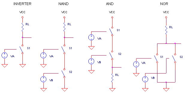
AND - Switches in Series OR - Switches in Parallel |
INVERTED - Pull-Up
Resistor NON-INVERTED - Pull-Down Resistor |
THE NAND GATE
So let's have a go at simulating the NAND gate. How do you describe its function? When both A and B are HI, the output is LO. Or stated another way - it's the AND function with an inverted output. The Boolean expression looks like
The circuit appears below. S1 and S2 in series create the AND function; RL in the pull-up position inverts the output. Defining the NAND gate as a subcircuit makes it easy to insert it into a few locations if you wish. The subcircuit nodes are listed in parenthesis. ( See Why Use Subcircuits? )
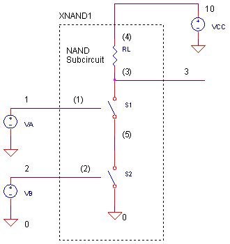
S1 and S2 are defined by RON = 10 Ω and ROFF = 1 MΩ. Compared to the other resistances in the circuit, these should look like an ideal switches. More on the SPICE switch below.
CIRCUIT INSIGHT Simulate the SPICE circuit named LOGIC_SW.CIR. VA and VB create two binary signals that form the sequence 00, 01, 10 and 11. VCC = +5V supplies power to the logic gate. Plot the inputs V(1), V(2) and the output V(3). For a clearer view, you might want to plot V(3) in a separate plot window. Does the output go LO when V(1) and V(2) are HI?
Note the finite rise and fall times of V(1) and V(2). You may have also noticed that the output V(3) quickly changes when the inputs pass through 2.5 V. This is the approximate logic threshold level defined for the SPICE switches.
OTHER GATES
You can test drive some of the other gates defined in SPICE file. Place an asterisk * in front of the NAND statement and call one of the other gates. Simulating the XNOR gate, for example, would like this.
*XNAND1 1 2 3 10 NAND
XNOR1 1 2 3 10 NOR
After running a simulation, plot the inputs V(1), V(2) and output V(3). Does the output NOR gate go LO when either A or B are HI?
HANDS-ON DESIGN Try your hand at creating a gate such as the OR function. It might be easier if you make a copy of an existing subcircuit, like the NOR gate, then change it as needed. As a design guide, refer to table at the top of the page.
3-INPUT GATES
HANDS-ON DESIGN What if your circuit calls for a three-input device? Just draw the three input circuit, label the nodes and create the SPICE netlist. The device and subcircuit definition for a three-input NAND gate might look something like
XNAND1 1 2 3 4 10 NAND3
.SUBCKT NAND3 1 2 3 4 5
* TERMINALS A B C OUT VCC
.
. (circuit goes here)
.
.ENDS
where nodes 1, 2, 3 = inputs, node 4 = output and node 5 = VCC. Remember to add a third input signal VC (creating a binary sequence 000, 001, ..., 111 using VA, VB and VC).
VC 3 0 PULSE(5V 0V 0NS 10NS 10NS 390NS 800NS)
and extend the simulation by a factor of two.
.TRAN 5NS 800NS
When you're ready to test your circuit, run a simulation, plot the inputs V(1), V(2), V(3) and the output V(4). You might get a better view by plotting V(4) in a separate plot window. Does the output go LO only when all inputs are HI?
ADDING GATE DELAY
You could run into trouble when running a transient analysis on devices with fast transitions. SPICE algorithms may fail under these conditions. This is especially true with complex circuits having feedforward or feedback paths. ( Like RS flip-flops created from NAND gates.) The solution is to sprinkle a little RC delay on the devices slowing the transitions enough to where SPICE successfully computes the simulation.
HANDS-ON DESIGN You can include 10 pF in the NAND gate output by adding the following statement in the subcircuit.
CL 3 0 10PF
Run a simulation and plot the output V(3). Can you see the slowed transitions at the output? You may have noticed the rising edge is slower than the falling edge. That's because the RC time-constant is defined by RL = 500 Ω ohms when the switch is OFF and RON = 10 Ω when the switch is ON.
FURTHER ADVENTURES
By combining gates, you can create more complex functions like the Exclusive-OR gate. Knowing the XOR output is 1 when (A,B) = (0,1) or (1,0), you can write the Boolean expression as
![]()
How can you wire up several gates (AND, OR and NOT) to accomplish the XOR function?
SIMULATION NOTES
S1 and S2 are voltage controlled switches. These handy SPICE components let you define the ON and OFF resistances and corresponding control voltages. Switches are defined by two statements: the device itself and its model.
S1 3 5 1 0 SW
.MODEL SW VSWITCH(VON=2.6 VOFF=2.4 RON=10 ROFF=1MEG)
Defining the term R(3,5) as the resistance between switch nodes 3 and 5, you can interpret the model as follows. If V(1,0) ≥ 2.6V then R(3,5) = 10 Ω. Similarly, if V(1,0) ≤ 2.4V then R(3,5) = 1 MΩ. Between the ON and OFF voltages, 2.4V ≤ V(1,0) ≤ 2.6V, the resistance varies continuously between RON and ROFF. (Using RON, ROFF, you could define a switch that turns OFF when the input goes HI.)
SPICE FILE
Download the file or copy this netlist into a text file with the *.cir extention.
LOGIC_SW.CIR - BASIC LOGIC GATES USING SWITCHES
*
VCC	10	0	5V
*
* INPUT A AND B, COUNT IN BINARY 0 - 3
VA	1	0	PULSE(5V 0V 0NS 10NS 10NS 90NS 200NS)
VB	2	0	PULSE(5V 0V 0NS 10NS 10NS 190NS 400NS)
*
XNAND1	1 2 3 10	NAND
*
*
* LOGIC GATE SUBCIRCUITS ******************************************
*
.SUBCKT NAND 1 2 3 4
* TERMINALS A B OUT VCC
RL	3	4	500
S1	3 5	1 0 	SW
S2	5 0	2 0 	SW
.ENDS
*
.SUBCKT AND 1 2 3 4
* TERMINALS A B OUT VCC
S1	4 5	1 0 	SW
S2	5 3	2 0 	SW
RL	3	0	500
.ENDS
*
.SUBCKT NOR 1 2 3 4
* TERMINALS A B OUT VCC
RL	3	4	500
S1	3 0	1 0 	SW
S2	3 0	2 0 	SW
.ENDS
*
.SUBCKT NOT 1 3 4
* TERMINALS A OUT VCC
RL	3	4	500
S1	3 0	1 0 	SW
.ENDS
*
*
.MODEL	SW	VSWITCH(VON=2.6 VOFF=2.4 RON=10 ROFF=1MEG)
*
* ANALYSIS **************************************************
.TRAN 	5NS  	400NS
*
* VIEW RESULTS
.PRINT	TRAN 	V(1) V(2) V(3)
.PROBE
.END
© 2002 eCircuit Center