Op Amp Bandwidth
CIRCUIT
|
|
|
Non-Inverting Amplifier
Inverting Amplifier |
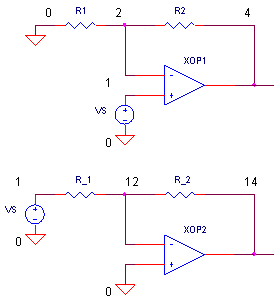
OP_BANDWIDTH1.CIR Download the SPICE file
Its all about speed - at least that's the focus of this topic. In an ideal world, an op amp responds instantly to a change in signal (audio, sensor, video, other). But in the real world, there's a limit on the highest frequency (bandwidth) and fasted edge your op amp can process. A few simple concepts provide insight into an amplifier's bandwidth. And knowing this can help you make better op amp and circuit choices.
NON-INVERTING VS. INVERTING SHOWDOWN
Here's a showdown between the two classic amplifiers. For the same gain, which amplifier has the greater bandwidth? We'll use a voltage gain of 2 for both circuits.
| Amp | Gain Rs |
Closed-Loop Gain GCL |
Noise
Gain GN |
Unity-Gain Freq, fu |
Bandwidth fc = fu / GN |
| Non-Inverting | R1 = 10 k R2 = 10 k |
(R1+R2)/R1 = +2 V/V | (R1+R2) / R1 = 2 | 10 MHz | 10 MHz / 2 = 5 MHz |
| Inverting | R1 = 10 k R2 = 20 k |
-R2/R1 = -2 V/V | (R1+R2) / R1 = 3 | 10 MHz | 10 MHz / 3 = 3.3 MHz |
The bandwidth champion is the non-inverting amplifier for the same absolute gain! However, as gains get larger, this bandwidth difference becomes smaller. Still, all other things being equal, the non-inverting amplifier has a bandwidth advantage. Why? Learn more below!
CIRCUIT INSIGHT
To get a gut feel, run an AC simulation of OP_BANDWIDTH1.CIR.
Set the resistors in
the non-inverting and inverting amplifiers to values in the table above. Plot
the AC output at V(4) and V(14). Did the non-inverting gain live up to
expectations?
THE REAL STORY OF GAIN
To understand bandwidth, we must understand the real gain equation. You've probably seen the ideal Closed-Loop voltage gain equation Gcl=vo/vs for a non-inverting amplifier.
But, what's the real story including the op amp's internal gain? It actually looks like this
where
A - open-loop gain - internal gain of the op amp itself.
β - feedback factor - how much of the output is fed back to the negative input
Here's the beauty of this equation. Check
out what happens to GCL if A is made large.
For A >> (R2+R1) / R1,
The bottom line? The gain is set by R1 and R2, not the op amp gain A! (This fact certainly simplifies op amp circuit design.) But the bigger take away is this: A can vary due to initial tolerances or temperature drift, but the voltage gain holds rock solid set by the resistor values!
BANDWIDTH
So what's the problem with the real gain equation? Although, A is large (+100,000) at lower frequencies, it falls at higher frequencies to well below unity (<<1). And when A drops near (R2+R1) / R1, GCL drops too. The frequency where GCL falls below the ideal gain is called the closed-loop bandwidth fc.
CIRCUIT INSIGHT
Run an AC simulation of OP_BANDWIDTH1.CIR.
The closed-loop gain
for this circuit is GCL = (10k+10k)/10k = 2 V/ V. Plot
the AC Response for the output at V(4) and open loop gain A using the equation V(4)/(V(2)-V(1)). To get
a clearer view, select log for the Y-Axis. For this particular op amp,
A has a DC gain of 100,000 V/V, then falls off above 100 Hz. What about GCL?
You can see that all is well as long as A >> 2. But when A drops close to
GCL,
the closed-loop gain takes a dive.
Note where GCL begins to drop. The frequency where the voltage falls to 0.707 of its DC value is the cutoff or -3 dB frequency, fc. ( Gain in decibels = 20∙log(0.707) = -3dB. )
HANDS-ON DESIGN Pick a higher gain. Choose R2 somewhere in the range of 10 k to 10,000 kΩ. Rerun the simulation. Yes, GCL looks great at low frequencies, but what happened to the bandwidth? Because GCL is essentially bounded by A, the bandwidth fc gets smaller for a higher gain! Life and circuit design are full of compromise, and gain versus bandwidth is a fine example.
Can you extend the bandwidth GCL?
Sure, select
an op amp with larger A. The op amp model simulates the DC gain A with
EGAIN 3 0 1 2
100K.
Increase the 100k by a factor of 10 or so. Or, you can increase the bandwidth
by decreasing RP1 or CP1 by a factor of 10. Run a new simulation. Did your
new op amp extend the bandwidth at V(4)?
NON-INVERTING BANDWIDTH
How can you predict the bandwidth at any gain? A simple equation gets you the answer.
fc = fu / GN
where
fu (Unity Gain Frequency) - the frequency where the open-loop gain A falls to unity (1V/V or 0dB).
GN (Noise Gain) - the gain from v+ to vo. Note: it's the inverse of the feedback factor β.
GN = vo/v+ = (R1 + R2) / R1 = 1/β
Why the name "noise gain"? Typically, noise is modeled as a voltage
source at the op amps's positive input v+. So the non-inverting
gain is used to calculate the resulting output. Does the noise gain equation look familiar? It
should!
The noise gain same as the closed-loop signal gain for the non-inverting amplifier
GN = GCL.
For example, a non-inverting amplifier having a fu = 10 MHz and R1 = R2 = 10k gives a closed-loop gain GCL = 2 and a noise gain of GN = 2. Calculating its bandwidth fc, we get
fc = fu / GN
= 10 MHz / 2
= 5 MHz
HANDS-ON DESIGN Run a few simulations with various voltage gains of OP_BANDWIDTH1.CIR. Plot the AC Response at the output at V(4) and A via the equation V(4)/(V(2)-V(1)). Adjust the gain by varying R2 and R1. You should be able to predict the bandwidth at V(4) for any of your chosen gains.
THE INVERTING AMPLIFIER
What about the inverting amplifier? The results are similar with a slight twist. Let's start with it's closed-loop gain equation - significantly different than the non-inverting gain.
where A is the internal gain and the feedback factor is
β = R1 / (R1+R2).
Note, the feedback factor, β = R1 / (R1+R2), is the same for inverting or non-inverting amplifier. That's because β is simply the gain of vo to the neg input (β = V- / Vo), just like the non-inverting amp.
Similar to the non-inverting amplifier,
when A is large, the ideal inverting gain is achieved
For A >> (R2+R1) / R1,
However, as frequency increases and A drops close to the ideal gain, GCL begins to drop. How do we predict this frequency where the gain falls off? Similar to the non-inverting amplifier we calculate
fc = fu / GN
The fc calculation also uses the noise gain. But here's the twist, the noise gain for the inverting amp is the same as the non-inverting amp!
GN = vo/v+ = (R1 + R2) / R1 = 1/β
For example, an op amp having a fu = 10 MHz and R1 = R2 = 10k gives an inverting gain of GCL = -1. However, the bandwidth is reduced by the noise gain GN = (R1 + R2) / R1 = 2 giving
fc = fu / GN
= 10 MHz / 2
= 5 MHz
Here's the disadvantage of the inverting amplifier:
signals are amplified
by the R2 / R1 ratio, but the bandwidth is knocked down by the larger (
R1+R2 ) / R1 ratio.
CIRCUIT INSIGHT
Try out the inverting amplifier in the OP_BANDWIDTH1.CIR.
Plot
the AC Response for the output V(14) and the op amp's internal gain
V(14)/V(12). A log plot on the Y-Axis can give a better view. The gain
should match the ideal -R2 / R1 as long as A is larger than (R1+R2)/R1.
HANDS-ON DESIGN Crank up the gain by choosing R2 somewhere in the range of 10 k to 10,000 kΩ. Rerun the simulation. For any gain, GCL should be bounded by A. Does the bandwidth get smaller as you increase gain?
NON-INVERTING VS. INVERTING AMPLIFIER
Now hopefully you can return to the opening showdown between the two classic amplifiers (top of page) armed with a better understanding of the results!
GAIN-BANDWIDTH-PRODUCT
The term fu is related to the Gain-Bandwidth-Product (GBP). Why? If we rearrange fc = fu / GN, we get
fu = GN x fc = GBP
Notice, that the product of GN (noise gain) and fc (closed loop gain) is a constant bounded by the Gain x Bandwidth Product!
What does this mean? You can't arbitrarily set the gain and bandwidth for a given op amp. Increase the gain GN, and the bandwidth fc will drop to keep GBP constant. Alternatively, if you need a higher bandwidth, then you must choose a lower gain. If you need both higher gain and bandwidth, you're out of luck with this device. You need to pick an op amp with a higher fu (or GBP) on its data sheet.
Please note, fu = GBP holds true for op amps with a single pole open-loop response. However, even for others with higher poles, the product is close enough fu ≈ GBP ,
BW AND RISE-TIME
Another way to measure circuit speed is how fast the amplifier responds to a step input. In the real world, the step input represents a quick brightness change in a video signal or the rising / falling edge of a clock signal. Run a .TRAN simulation and plot V(4) and V(14). How much faster does the non-inverting output reach 90% of its final value compared to the inverting output?
SIMULATION NOTES
Another critical
parameter that limits bandwidth is Max Slew Rate.
For a more detailed description of the op amp, see the Basic Op
Amp Model.
For a quick review of subcircuits, check out Why Use Subcircuits?
SPICE FILE
Download the file or copy this netlist into a text file with the *.cir extension.
OP_BANDWIDTH1.CIR - OPAMP BANDWIDTH
*
VS	1	0	AC 1V	PWL(0US 0V   0.01US 1V  100US 1V)
*
*
* NON-INVERTING AMPLIFIER
R1	2	0	10K
R2	2	4	10K
XOP1	1 2	4	OPAMP1
*
* INVERTING AMPLIFIER
R_1	1	12	10K
R_2	12	14	10K
XOP2	0 12	14	OPAMP1
*
*
* OPAMP MACRO MODEL, SINGLE-POLE
* connections:      non-inverting input
*                   |   inverting input
*                   |   |   output
*                   |   |   |
.SUBCKT OPAMP1      1   2   6
* INPUT IMPEDANCE
RIN	1	2	10MEG
* DCGAIN =100K AND POLE1=1/(2*PI*RP1*CP1)=100HZ
* GBP = DCGAIN X POLE1 = 10MHZ
EGAIN	3 0	1 2	100K
RP1	3	4	1000
CP1	4	0	1.5915UF
* OUTPUT BUFFER AND RESISTANCE
EBUFFER	5 0	4 0	1
ROUT	5	6	10
.ENDS
*
*
* ANALYSIS
.AC 	DEC 	5 10 100MEG
*.TRAN 	0.01US  0.5US
*
* VIEW RESULTS
.PROBE
.END
top
© 2002-2024 eCircuit Center