Basic Op Amp Model
CIRCUIT
OPMODEL1.CIR Download the SPICE file
One of the challenges of simulating op amp circuits is modeling the op amp itself. How is that accomplished? There's a couple of ways. You can create a circuit of many transistors, resistors and caps that closely replicate the internals of an op amp. Or, you can create a simpler model that reproduces the basic behavior of the op amp. The benefit of the simpler model is one that uses less components and typically simulates faster. As you begin to look at more complex or subtle behaviors, you can create a more complex op amp model.
To simulate more complex behaviors, check out the Intermediate Op Amp Model.
For a description of all available op amp models, see Op Amp Models.
Solve 10 Op Amp Design Issues using Custom LTSPICE MODELS.
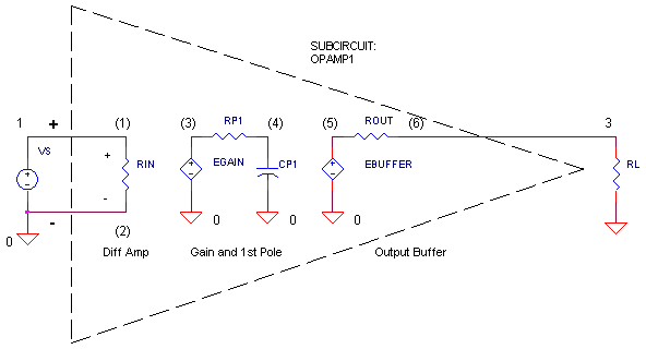
OP AMP MODEL
What are the three basic stages of an op amp? The
circuit above shows
1) A differential amplifier with high voltage gain RIN, EGAIN
2) A single-pole low-pass filter frequency RP1, CP1
3) An output buffer (unity gain). EBUF, ROUT
Why a differential amp with high gain?
Open-loop gain is defined as the gain with no external feedback resistors – i.e. the loop from output to input is open. On the other hand, the closed-loop gain is typically defined by two external resistors. But, the closed-loop gain holds true only if the open-loop gain (no external resistors) is much larger than the closed-loop gain. Therefore, manufacturers of op amps strive to make this gain as large as possible (>10000 V/V).
Why a low-pass filter?
Too much open-loop gain at high frequencies may cause an op amp to ring or oscillate. Bad news! To prevent oscillation, the low-pass filter rolls off the open-loop gain to less than 1 (unity) at higher frequencies.
Why an output buffer?
The gain and filter stages are typically low power stages. The output buffer provides output current drive and isolates the gain and low-pass filter components from the output.
If you're designing a precision amplifier, you can use the model to see how open loop gain affects accuracy. If you're designing a high-speed amplifier, you can determine your circuit's bandwidth.
OPEN-LOOP FREQUENCY RESPONSE
The open-loop response gives you some powerful insight
into the op amp’s performance. Open-loop means NO feedback; the response of
the “naked” op amp. Two important features are
1. DC Gain, Aol – the open-loop gain at DC. This gain is provided by the voltage controlled voltage source EGAIN. A higher gain means a higher bandwidth and more gain accuracy when you close the loop with feedback resistors.
2. First-Pole Frequency, fp1 – the frequency where the open-loop gain begins to fall. A simple RC creates this low-pass filter.
fp1 = 1/( 2 * π * RP1 * CP1)
3. Unity-Gain Frequency, fu - the frequency where the open-loop gain falls to 1 V/V. The bigger the fu, the faster your op amp responds. What determines this frequency? It’s a function of the DC Gain Aol and fp1.
fu = Aol x fp1
Let’s create a SPICE model that we can take out for a spin. First, we'll specify it.
| Op Amp Specification | ||
| Aol = 100k V/V | DC Gain | |
| fu = 10 MHz | Unity Gain Frequency, or (GBP) Gain Bandwidth Product |
Then, calculate the components.
| SPICE Model Design | ||
| Choose | RP1 = 1k | |
| Calculate | K_EGAIN = Aol = 100k (Set EGAIN to this value.) | |
| fp1 = fu / Aol = 10MHz / 100k = 100 Hz. | ||
| CP1 = 1/(2*pi*fp1*RP1) = 1.59 uF |
What about RIN and ROUT? Sometime these values can be read right from the data sheet. As a default, I typically set them to RIN=1e12 and ROUT=100 ohms. As a convenience, we'll define this op amp model as a subcircuit.
CIRCUIT INSIGHT
The op amp is driven by AC source VS. There are no feedback
resistors here – its running open-loop. Try out the model by running a
simulation and plotting the AC magnitude
VM(3). Can you see the DC gain =
100k V/V and the first-pole at fp1 = 100 Hz? What is the unity gain
frequency? Try changing the Y-Axis
to a log scale to get a better view at high frequencies. If your
plotting in dB, the unity-gain level is 0 dB.
HANDS-ON DESIGN Suppose you need to model a faster op amp with the same DC gain but a higher unity-gain frequency fu. Choose a higher fu such as 50 MHz, then solve for a new fp1. For example,
Choose fu = 50 MHz.
Calculate fp1 = fu / DCGAIN = 50 MHz / 100 k = 500 Hz
CP1 = 1/( 2 * π * 1k * 500 Hz) = 0.318 uF.
Try out your new op amp model. Did the magnitude VM(3) hit the unity-gain around 50 MHz?
CLOSED-LOOP TEST
Enough open-loop analysis already! Let’s see strap some
feedback resistors around this device and see how it works in a closed-loop.
All you need is to add the following resistors and change the XOP statement.
R1 1 0 10K
R2 2 3 10K
XOP 1 2 3 OPAMP1
Then, run a Transient Analysis (Time domain) using the .TRAN statement. The op amp is driven by 1V step function defined by the PWL source in the VS statement. With R1 = R2 = 10k, the gain should be R2/R1+1 = 2 V/V.
CIRCUIT INSIGHT Run a simulation and plotting the input V(1) and output V(3). You should see the output rise to 90% of its final value rather quickly (<1us). To see the exact output, place a cursor on V(3) and see how close it gets to 2.000 V. How does the DC gain (Aol) affect closed-loop gain accuracy? Start dropping the DC gain (100k) in the EGAIN statement factors of 10x: 10k, 1k, …. At what point does the output drop noticeable from 2.000 V?
Try lowering the fp1 by setting RP1 or CP1 to a higher value. This should consequently lower fu and slow down the rise time. Run a simulation and check out how fast the output responds.
CURRENT SOURCE MODEL
Here’s an important alternative to creating the same
behavior using a current source instead of a voltage source. This model
lends itself to easily adding more behaviors such as max slew rate or
voltage limits. The idea is simple - replace the series combination of a
voltage source and a resistor with a parallel combination of current source
and a resistor. Both models create a voltage at V(3)based on the input
voltage V(1,2) multiplied by the DCGAIN.
G1 0 3 1 2 100
RP1 3 0 1k
CP1 4 0 1.5915UF
Basically, G1’s current flows into RP1 creating V(3).
In this model, the DC gain (Aol) defined by both RP1 and KG1 (the gain of G1 in
units of A/V).
Aol = KG1 * RP1
The fp1 and RC calculations are the same. Let’s create the current source based model for the op amp defined above: Aol = 100k V/V and fu = 10 MHz.
| SPICE Model Design | ||
| Choose | RP1 = 1k | |
| Calculate | KG1 = Aol / RP1 = 100k / 1k = 100 (Set G1 gain to this value.) | |
| fp1 = fu / Aol = 10MHz / 100k = 100 Hz. | ||
| CP1 = 1/(2*pi*fp1*RP1) = 1.59 uF |
Try replacing EGAIN in the voltage model with G1 and place RP1 in parallel with CP1. Adjust the values of RP1 and CP1, then rerun the simulation. The results should be identical.
PHASE SHIFT
CIRCUIT INSIGHT
So far we’ve looked at the gain of the op amp. At some point, you may need to know the phase shift
(time delay) as well. To check out the phase shift, add another plot to the
window, then, add trace VP(3)
where the P
tells SPICE to display the Phase.
A maximum of -90 degrees of phase shift should occur beyond the first pole
fp1.
What’s the big deal about phase anyway? Turns out, the phase shift (and gain) of the signal in a feedback circuit reveals how well a circuit performs. Too much negative phase can cause an amplifier circuit to overshoot, ring or even oscillate. Knowing the phase shift will help you fix the problem. On the other hand, if you’re designing an oscillator, you’ll intentionally add the right amount of negative phase at the right frequency. More on these topics in Op Amp Feedback Analysis.
OP AMP CIRCUITS
This op amp model is used inside op amp circuits in this site: Inverting Amplifier, Non-Inverting Amplifier, etc. Go ahead and turbo-charge some of the op amps by upping the Unity-Gain Frequency of the model and checking out its effect on the closed-loop bandwidth (with feedback components) of the amplifier.
SIMULATION NOTE
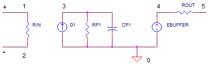
The op amp model is created from several simple SPICE
devices. The differential input and DCGAIN stage are implemented by a
Voltage-Controlled Voltage Source (VCVS) named EGAIN. The device
EGAIN 3 0 1
2 100K
follows the syntax
E{name} {+output} {-output} {+control}
{-control} {gain}
which creates a voltage source having positive and
negative output terminals at nodes 3 and 0. The source is controlled by the
voltage at positive and negative sense leads 1 and 2. This voltage is then
multiplied by the gain 100k and applied at the output terminals. The output
buffer EBUFFER is simply another VCVS.
SPICE makes three other controlled sources available: a Current-Controlled Voltage Source (CCVS), a Voltage-Controlled Current Source (VCCS) and Current-Controlled Current Source (CCCS). Check them out at the SPICE Command Summary.
RELATED TOPICS
To simulate more complex behaviors, check out the
Intermediate Op Amp Model.
See a description of all available op amps at
Op Amp Models.
For a quick review of subcircuits, check out
Why Use Subcircuits?
Get a crash course on SPICE simulation at
SPICE Basics.
To see how open-loop gain and bandwidth influence closed-loop bandwidth,
see Op Amp
Bandwidth.
This op amp model can be used many of the op amp
circuits available from the Circuit
Collection page.
SPICE FILE
Download the file
or copy this netlist into a text file with the *.cir
extention.
OPMODEL1.CIR - OPAMP MODEL SINGLE-POLE
*
VS	1	0	AC	1  PWL(0US 0V  0.01US 1V)
XOP	1 0	3	OPAMP1
RL	3	0	1K
*
* OPAMP MACRO MODEL, SINGLE-POLE
* connections:      non-inverting input
*                   |   inverting input
*                   |   |   output
*                   |   |   |
.SUBCKT OPAMP1      1   2   6
* INPUT IMPEDANCE
RIN	1	2	10MEG
* DC GAIN=100K AND POLE1=100HZ
* UNITY GAIN = DCGAIN X POLE1 = 10MHZ
EGAIN	3 0	1 2	100K
RP1	3	4	1K
CP1	4	0	1.5915UF
* OUTPUT BUFFER AND RESISTANCE
EBUFFER	5 0	4 0	1
ROUT	5	6	10
.ENDS
*
* ANALYSIS
.AC 	DEC 	5 1 100MEG
*.TRAN 	0.05US  2US
* VIEW RESULTS
.PROBE
.END
© 2002-2024 eCircuit Center