Op Amp Input Bias Current
CIRCUIT
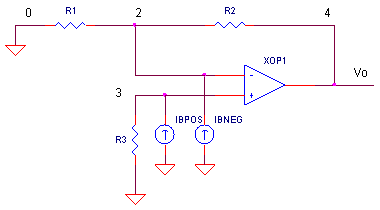
OP_IBIAS.CIR Download the SPICE file
One of the golden rules of op amp analysis says this: no current flows into either input terminal. This concept is key for analyzing an amplifier's signal gain. However, in reality, a small current flows into both inputs to bias the input transistors. Unfortunately, this bias current gets converted into a voltage by the circuit's local resistors and amplified right along with the signal. The result is an output error in your circuit. What can you do about it? A clever choice of resistor values can help you cancel most of the output error. .
INPUT BIAS CURRENT
Depending on the type of input transistor, the bias current can flow in or out of the input terminals. The input current is modeled as current sources, Ib+ and Ib-, in parallel with the positive and negative input terminals. How big is this current? The magnitudes can range from μA down to pA. Generally speaking, JFET or CMOS op amps have smaller bias currents than BJT types.
Input bias currents of early op amps were relatively large and equal.
Ib+ = Ib- = Ib
Modern op amps have smaller Ib+ and Ib- owed to a clever circuit technique called input bias current cancelation. However, their differences are more pronounced described by the input offset current.
Iboff = Ib+ - Ib-
You can rewrite the current into each input as
Ib+ = Ib +Iboff/2
Ib- = Ib - Iboff/2
where Ib is the average of the two currents.
OUTPUT ERROR
Is the circuit shown above an inverting or non-inverting amplifier? The answer is yes, both! With the input signal source set to 0 V ( shorted ), the inverting and non-inverting amplifiers look the same. What kind of undesirable voltage does the bias current create in your circuit?
Effect of Ib+ on Vo
Vo = Ib+ ∙ R3 ∙ ( R2 / R1 + 1 )
This is easy to understand. Ib+ flowing into R3 produces a voltage at the + input. Treating it like any other voltage at this terminal, the op amp amplifies it according to the non-inverting gain equation.
Effect of Ib- on Vo
Vo = - ( Ib- ∙ R2 )
Just like the transimpedance (current-to-voltage) amplifier, the output voltage is simply the input current times the feedback resistor.
What are the equations above telling us about resistor choice? For a given op amp, the smaller the resistor values, the smaller the errors. However, certain design goals, like low power, may force high resistor values. As usual, the end result is a compromise between competing design parameters.
CIRCUIT INSIGHT
Run a simulation of OP_IBIAS.CIR.
To look at the effect
of Ib+ only, set the current sources to IBPOS = 100 nA
and IBNEG = 0 nA. With R1 = 10k, R2 =
10 k and R3 = 10k, you'd expect to see an output error of 100 nA
∙ 10 k ∙
(10k/10k + 1 ) = +2 mV at V(4).
Next, let's look at Ib- only. Set IBPOS = 0 nA and IBNEG = 100 nA. In this case you'd expect to see an output error of - 10k ∙ 100 nA = -1 mV.
Try scaling the resistors up and down to values like 100k or 1k. Run a new simulation. Do the errors scale along with the resistors? Also, notice that the errors for Ib+ and Ib- are opposite polarity! Maybe we can use this fact to make the errors from both currents cancel each other.
INPUT BIAS CANCELLATION
Currents Ib+ and Ib- create errors of opposite polarity. The question now is this: can we choose a magical value of R3 to force the errors caused by both bias currents to cancel each other? First, let's describe our goal mathematically. We would like the errors from both sources to be equal and opposite to one another. To do so, just take the two error equations above and set them equal to each other. Also, assume that the bias currents are equal Ib+ = Ib- = Ib.
Ib ∙ R3 ∙ ( R2 / R1 + 1 ) = Ib ∙ R2
Next, solve for R3 in terms of R1 and R2.
R3 = ( R2 ∙ R1 ) / ( R1 + R2 ) = R1 || R2
The solution is clear, choose R3 equal to the parallel combo of R1 and R2, and the bias current errors will cancel!
HANDS-ON DESIGN Set both IBPOS and IBNEG equal to 100nA. With R1=10k, R2=10k, set R3=R1||R2 = 5k, then run a simulation of OP_IBIAS.CIR. Did your new choice of R3 reduce the output error at V(4) to 0V?
INPUT OFFSET CURRENT
Not to burst the bubble, but a clever choice of R3 doesn't mean all of the error is gone. As shown above, the input currents are not exactly matched. Suppose Iboff = 20 nA. To see the effect of this offset, set IBPOS = 110nA and IBNEG = 90 nA. With R1=10k, R2=10k and R3=R1||R2=5k, run a simulation. How much residual error has popped up at V(4) due to the input offset current?
Many of today's application notes say to forego the R3 cancellation technique and simply minimize the resistance magnitudes. However, it's best to evaluate each amplifier circuit and specific device bias currents on their own.
TEMPCO
The input bias current will change ∆I (current drift) with a change in temperature ∆T. This error is typically an exponential function, however, you can approximate a linear one from a an Ibias plot from the data sheet.
Ibias_TC = ∆Ibias / ∆T (A/deg C)
For an with tempco of 1nA / deg C, what is the drift over, say ∆T = 10 deg C?
Ibias = Ibias_TC · ∆T
= (1nA / deg C) · 10 deg C
= 10nA
INPUT OFFSET VOLTAGE
Input bias current is not the only undesirable characteristic of the op amp's input. (See Op Aamp Input Offset Voltage )
SPICE FILE
Download the file or copy this netlist into a text file with the *.cir extention.
OP_IBIAS.CIR - OPAMP INPUT BIAS CURRENT
*
* AMPLIFIER CIRCUIT
*
R1	0	2	10K
R2	2	4	10K
R3	3	0	10K
XOP1	3 2	4	OPAMP1
*
* OPAMP INPUT BIAS CURRENT
IBPOS	0	3	DC	100NA
IBNEG	0	2	DC	100NA
*
*
* OFFSET ADJUSTMENT
* POTENTIOMETER DIVIDER - VPOT
*VPOT	10	0	PWL(0MS -0.2V   10MS 0.2V)
*R4	10	2	1MEG
*
*
* OPAMP MACRO-MODEL, SINGLE-POLE
* connections:      non-inverting input
*                   |   inverting input
*                   |   |   output
*                   |   |   |
.SUBCKT OPAMP1	     1   2   6
* INPUT IMPEDANCE
RIN	1	2	10MEG
* GAIN BW PRODUCT = 10MHZ
* DC GAIN (100K) AND POLE 1 (100HZ)
EGAIN	3 0	1 2	100K
RP1	3	4	1K
CP1	4	0	1.5915UF
* OUTPUT BUFFER AND RESISTANCE
EBUFFER	5 0	4 0	1
ROUT	5	6	10
.ENDS
*
* ANALYSIS
.TRAN 	0.1MS  10MS
* VIEW RESULTS
*.PRINT	TRAN 	V(4)
.PROBE
.END
© 2002 - 2025 eCircuit Center