Op Amp Integrator
CIRCUIT
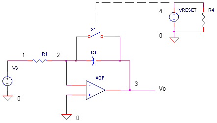
OPINT.CIR Download the SPICE file
The integrator basically works like this: whatever current I you get flowing in R1, gets integrated across capacitor C1. The output voltage Vo is simply the voltage across C1.
One great application of the integrator is generating a ramp voltage. You can do this by placing a fixed voltage at VS that forces a constant current through R1. The capacitor then integrates this current creating a ramping voltage.
The integrating action is just like a garden hose running water at a constant rate causing the level in a bucket to rise steadily. The smaller the diameter bucket (smaller capacitor), the faster the increase in water level (greater voltage). The switch is needed to discharge the capacitor (empty the bucket) at the end of a ramping cycle.
RAMP GENERATOR
The circuit essentially integrates the input current Is = VS / R1 across capacitor C1. After a time interval T, the output is the capacitor voltage described by

If you apply a constant voltage at VS, the output voltage increases steadily (ramp). You can predict the ramp's voltage at any time T by the simplified equation
![]()
CIRCUIT ANALYSIS Try the circuit. What is the output voltage V(3) after 100us? With VS= -1, R1=10k and C1 = 1nF, the output should be Vo = -1/1nF x (-1/ 10k) x 100us = 1V.
Look at the switch control voltage VRESET at V(4). VRESET turns the switch OFF (VRESET=0V) and ON (VRESET=5V). Switch S1 is initially OFF. After 100us, S1 turns ON discharging the capacitor for 10us. Then, the ramping cycle begins again.
HANDS-ON DESIGN Design a circuit that ramps faster or slower than the original circuit. The equation above tells you that you can change VS, R1 or C1 to achieve your goal. (Example: For a slower ramp, make R1 greater than its initial value. This cuts the current through R1 decreasing the ramp rate. ) You may have noticed that this is an inverting circuit; a negative VS creates a positive output. Need to create a create a negative ramp? Apply a positive VS.
SWITCH RESISTANCE
How important are the ON and OFF resistances of the switch in this application? Return the circuit to its original values (R1=10k, C1=1000pF, and VS=-1).
CIRCUIT INSIGHT Suppose you had a switch with an OFF resistance that‘s too small. What would happen to ramp voltage? Reduce the OFF resistance from 10MEG to a smaller value like 1MEG by modifying the switch model statement
.MODEL SRES VSWITCH(VON=0 VOFF=5 RON=100 ROFF=1MEG)
Try the circuit and plot the output V(3). Did the output reach your expected value? A smaller ROFF may discharge C1 significantly during the ramping interval.
What about an ON resistance that’s too large during the reset interval? Return ROFF to its initial value and increase RON from 100 to 1000.
.MODEL SRES VSWITCH(VON=0 VOFF=5 RON=1000 ROFF=10MEG)
Run the circuit. Did capacitor C1 discharge fully in the reset interval? What happens if RON is even larger like 10000?
SIMULATION NOTE
SPICE’s source statement named PULSE is a convenient way to generate a repeating pulsed waveform according to syntax
PULSE( {v1} {v2} {tdelay} {trise} {tfall} {width} {period} )
So the statement
VRESET 4 0 PULSE(0V 5V 0 0.1US 0.1US 100US 110US)
creates a repeating pulse from VRESET that’s defined by 0V for 100us and 5V for 10us for a total period of 110us. The rise and fall times are 0.1 us.
SPICE FILE
Download the file or copy this netlist into a text file with the *.cir extention.
OPINT.CIR - OPAMP INTEGRATOR
*
* CONTROL VOLTAGE FOR S1
VRESET	4	0	PULSE(0V 5V 0 0.1US 0.1US 100US 110US)
R4	4	0	1MEG
*
* INPUT VOLTAGE
VS	1	0	DC	-1
*
R1	1	2	10K
C1	2	3	1000PF
S1	2 3	4 0 	SRES
XOP	0 2	3	OPAMP1
*
.MODEL	SRES	VSWITCH(VON=0 VOFF=5 RON=100 ROFF=10MEG)
*
* OPAMP MACRO MODEL, SINGLE-POLE
* connections:      non-inverting input
*                   |   inverting input
*                   |   |   output
*                   |   |   |
.SUBCKT OPAMP1      1   2   6
* INPUT IMPEDANCE
RIN	1	2	10MEG
* GAIN BW PRODUCT = 10MHZ = DCGAIN x POLE1
* DC GAIN (100K) AND POLE 1 (100HZ)
EGAIN	3 0	1 2	100K
RP1	3	4	1K
CP1	4	0	1.5915UF
* OUTPUT BUFFER AND RESISTANCE
EBUF	5 0	4 0	1
ROUT	5	6	10
.ENDS
*
* ANALYSIS
.TRAN 	1US  	220US
.PROBE
.END
© 2002 eCircuit Center