Single-Supply AC Inverting Op Amp
CIRCUIT
OPINV_SS.CIR Download the SPICE file
Here's one challenge of today's electronics: if it's portable, it likely to be battery powered, and your circuit must be designed to perform in a single-supply world.
The key to single-supply design is in remembering that voltage potentials are meaningful only when taken relative to other potentials. For an op amp circuit, the bottom line is this: the signal should be somewhere around mid supply. The table below compares the potentials of a dual versus single supply design.
| power | pos supply pin | signal reference | neg supply pin | |
| Dual Supply | +5V | 0V | -5V | |
| Single Supply | +10V | +5V | 0V |
In both cases, the signal is centered around mid supply. Your design quest for single-supply is to amplify the signal while also biasing the signal at the mid-point voltage.
DUAL NATURE
As with many AC circuits, we can take advantage of their split personality: the DC Bias side and the AC Operation side. The circuits below shows its dual nature; one at DC (caps opened) and the other at AC (caps shorted.)
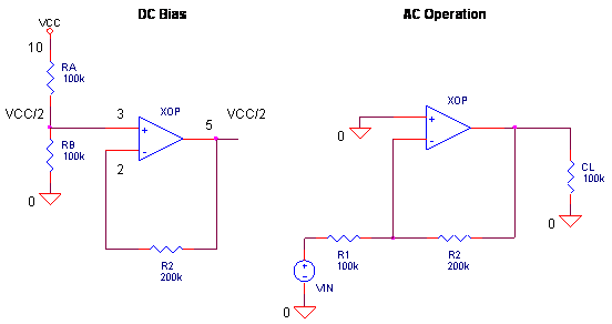
At DC the circuit becomes a simple voltage follower with its input/output at VCC/2 - the mid-supply bias level! At AC the circuit looks like your basic inverting amplifier described by the gain equation
![]()
AC INVERTING AMP
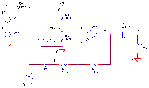
CIRCUIT INSIGHT Test drive the SPICE file OPINV_SS.CIR. A +5V source powers this circuit. For the Transient Analysis, plot the amplifier's input V(4) and output V(5). The output should be a combination of the mid-supply bias voltage (+2.5 V) and the AC signal amplified by a factor of -2.
HANDS-ON DESIGN You can change the gain by choosing a new value for R2. (Example: Choose R2 = 15k and calculate Vo = -1 x 10k / 10k = -1.) Edit the file with your new R2 value. Save the file and run a new simulation. Is the output swing at V(5) what you expected? If you wish, view the AC coupled input / output signals at V(1) and V(6) to see the sinewaves centered around 0V.
Here's an example of how an unquestioned simulation can lead to misleading results. What happens if you designed the above circuit with VCC/2 = +2.5V, VIN=1 Vpeak and GAIN= -5 The output would swing from +7.5 V to - 2.5V. Impossible for a single-supply circuit running from only +5 V! You should compare the output to the max output swing in an op amp's data sheet, or, get a more complex SPICE model that includes the output swing limits.
REDUCING NOISE
DANGER! The bias circuit opens up your amplifier to an undesirable signal: power supply noise. As you can see, the supply line has a direct line to your amplifier via the RA, RB divider. Any noise on this line directly disturbs output. How? The op amp's positive input to output pin is essentially the non-inverting amplifier configuration! The op amp dutifully amplifies any signal by (1 + R2/R1). The fix is easy. Place a decoupling capacitor to short any disturbances at the RA, RB divider output.
HANDS-ON DESIGN Let's throw a little noise (45 kHz, possibly from a switching power supply) onto the supply line by changing the noise generator from a 0V peak to a 0.2V peak voltage ( VNOISE 10 12 SIN(0V 0.2VPEAK 45KHZ) ). Now, simulate the amplifier. For the Transient Analysis, plot the input V(4), output V(5), supply V(10), and bias voltage V(3). What happened? The output is unacceptable! But you know the fix - increase CB until the 45 kHz is decoupled from the circuit. How large a value of CB do you need to squash the noise?
BANDWIDTH
Over what frequency range can you use this amplifier? The “AC 1” in the VS statement generates a voltage source of 1VRMS for the AC (frequency) sweep analysis. To check the response of the entire amplifier, sun a simulation and plot the AC results at V(6).
CIRCUIT ANALYSIS What are the lower, fL ,and upper, fU, cutoff frequencies of the amplifier? These are the points where the gain falls to 0.707 of the midband gain. For example, if your midband gain is 2, your cutoff frequencies occur where the gain decreases to 2 x 0.707 = 1.414 V/V. The bandwidth of your circuit is simply fBW = fU – fL.
What determines the shape of the frequency response? The table below shows the effective filters that define this circuit.
| filter | components | |
| high-pass | C1, R1 | |
| high-pass | CL, RL | |
| low-pass | op amp bandwidth |
HANDS-ON DESIGN Suppose your application must pass 10 kHz but ignore a 60 Hz interference. Does the bandwidth of this amplifier include 60Hz? Reduce either C1 or CL to reduce the response of your circuit at 60Hz.
SPICE FILE
Download the file or copy this netlist into a text file with the *.cir extention.
OPINV_SS.CIR - OPAMP INVERTING AMP, SINGLE-SUPPLY
*
* INPUT VOLTAGE
VIN	1	0	AC	1	SIN(0V  1VPEAK  10KHZ)   ; SIN(VOFFSET  VPEAK  FREQUENCY)
*
* VCC/2 BIAS VOLTAGE
RA	10	3	100K
RB	3	0	100K
CB	3	0	0.1NF
*
* INVERTING AMP
C1	1	4	0.1UF
R1	4	2	100K
R2	2	5	200K
XOP	3 2	5	OPAMP1
*
* OUTPUT LOAD
CL	5	6	0.1UF
RL	6	0	100K
*
*
* SUPPLY VOLTAGE (5 VDC) WITH NOISE SOURCE (OVPEAK INITIAL)
VDC	12	0	5VDC
VNOISE	10	12	SIN(0V  0VPEAK  45KHZ)     ; SIN(VOFFSET  VPEAK  FREQUENCY)
*
*
* OPAMP MACRO MODEL, SINGLE-POLE
* connections:      non-inverting input
*                   |   inverting input
*                   |   |   output
*                   |   |   |
.SUBCKT OPAMP1      1   2   6
* INPUT IMPEDANCE
RIN	1	2	10MEG
* DC GAIN (100K) AND POLE 1 (100HZ)
EGAIN	3 0	1 2	100K
RP1	3	4	1K
CP1	4	0	1.5915UF
* OUTPUT BUFFER AND RESISTANCE
EBUFFER	5 0	4 0	1
ROUT	5	6	10
.ENDS
*
* ANALYSIS
.TRAN 	0.001MS  0.2MS
.AC 	DEC 	5 10 100MEG
*
* VIEW RESULTS
.PRINT	TRAN 	V(4) V(5)
.PRINT	AC 	VM(6)
.PROBE
.END
© 2002 eCircuit Center