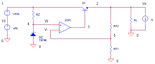
Op Amp Regulator with Series-Pass Transistor
CIRCUIT
OPREG.CIR Download the SPICE file
What is the function of a voltage regulator circuit? It’s basically this - maintain a precise voltage regardless of the current drawn by the load. Three basic components are needed to achieve good voltage regulation.
1. A precision reference (zener diode) to set the output voltage.
2. A muscle component (transistor) to deliver the required current.
3. An automatic controller (opamp) to adjust the transistor drive. The “prime directive” of the op amp is to adjust the base drive of Q1 delivering the required load current while keeping the output voltage at a fixed value.
OUTPUT VOLTAGE
Resistors RF1 and RF2 feed a fraction of the regulator output Vo to the op amp's negative input V-. The op amp then adjusts the drive to Q1 such that V- is equal to the zener voltage Vz. When this occurs, the output voltage is related to the zener voltage through the RF1, RF2 divider by
![]()
With the zener voltage at about 3V and RF2=10k, RF1=5K, the output voltage should be 3 x (1+10/5) = 9V. Run a simulation. What is the output voltage at V(2)?
HANDS-ON DESIGN Suppose you’re asked to design a 12V regulator. What value of RF2 would you need with Vz = 3V? Choose a new RF2 and test drive your circuit.
LOAD REGULATION
How well does the regulator perform? One test is to apply a change in the load current and see how well the regulator maintains its output voltage.
Current source IL generates a 1A pulse starting at 10ms and ending at 20ms. Place IL in the circuit by removing the "*" at the beginning of the IL statement. Run a simulation and plot the load current by adding trace I(IL) to the plot window.
The output should not change much except for the appearance of 2 small spikes. These spikes show that the regulator takes some finite time to respond when the load current changes.
CIRCUIT INSIGHT Want to see the automatic controller (op amp) in action? Plot the Q1 base voltage V(3) to see the op amp increase the transistor on-voltage when the during the 1A pulse. You can also see the op amp achieve its prime directive of maintaining V- = Vz by plotting V(4) and V(5).
LINE REGULATION
How well does the regulator hold the output voltage as the input voltage changes? The input voltage is a combination of VIN (DC source at 15V) and VS (AC sinewave currently set to 0V peak). To test the regulators line regulation, set VS to 1V peak by editing the VS statement to look like
VS 1 10 SIN(0 1 1KHZ)
Run a simulation and check how much variation appears at V(2). What causes these variations? One factor is the change in zener voltage V(4) due to a change at V(1). As V(1) varies, the current through RZ and consequently the zener diode voltage also varies.
SIMULATION NOTE
There are two semiconductors modeled here, zener diode D1N746 and transistor Q1. The diode parameters,(Is=5u Rs=14 Bv=2.81 Ibv=5u), came from the manufacturer’s web site. Actually there are more parameters than these four listed. The unlisted ones get set to their default parameters. For the simple transistor Q1 used, all of the default parameters are used except the current gain BF = 100.
CIRCUIT INSIGHT You can view Q1’s base current by adding IB(Q1) to the plot window. How much base current is required during the 1A draw of the load? The op amp supplies this current to the transistor. However, many op amps can only deliver about 10mA! If Q1 is asking for more, you may need to get an op amp with more current output muscle or a transistor with greater current gain BF. Set BF to a higher value like 200 and check IB(Q1) during the 1A load pulse.
SPICE FILE
Download the file or copy this netlist into a text file with the *.cir extention.
OPREG.CIR - OPAMP VOLTAGE REGULATOR W/ SERIES-PASS TRANSISTOR
*
* INPUT VOLTAGE (VSIN FOR TEST ONLY)
VIN	10	0	DC	15
VSIN	1	10	SIN(0 0 1KHZ)
* SERIES TRANSISTOR
Q1	1 3	2	QNOM
* REFERENCE VOLTAGE
RZ	1	4	5K
DZ	0	4	D1N746
* OPAMP CONTROLLER
XOP1	4 5	3	OPAMP1
RF2	2	5	10K
RF1	5	0	5K
* LOAD
RL	2	0	100
*IL	2	0	PWL(0 0  10MS 0   10.1MS 1   20MS 1   20.1MS 0   30MS 0)
*
.model	QNOM	NPN(BF=100)
.model	D1N746	D(Is=5u Rs=14 Bv=2.81 Ibv=5u)
*
* * OPAMP MACRO MODEL, SINGLE-POLE
* connections:      non-inverting input
*                   |   inverting input
*                   |   |   output
*                   |   |   |
.SUBCKT OPAMP1      1   2   6
* INPUT IMPEDANCE
RIN	1	2	10MEG
* GAIN BANDWIDTH PRODUCT = 10MHZ
* DC GAIN (100K) AND POLE 1 (100HZ)
EGAIN	3 0	1 2	100K
RP1	3	4	1K
CP1	4	0	1.5915UF
* OUTPUT BUFFER AND RESISTANCE
EBUFFER	5 0	4 0	1
ROUT	5	6	10
.ENDS
*
* ANALYSIS
.TRAN	0.05MS 30MS
* VIEW RESULTS
.PRINT TRAN	V(2)
.PLOT	TRAN    V(2)
.PROBE
.END
© 2002 eCircuit Center