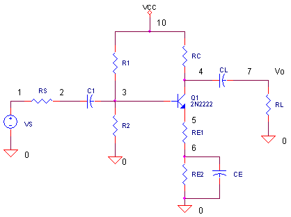
Common Emitter Transistor Amplifier
CIRCUIT

TRCE.CIR Download the SPICE file
Here’s a classic circuit that’s still an essential building block of circuits today, both IC and discrete.
VOLTAGE GAIN
Suppose you’re asked to design a transistor amplifier for a voltage gain of 3. The gain from the base to the collector can be approximated by the collector resistance over the emitter resistance.
![]()
where RC’ is the AC resistance seen by the collector, RC|| RL, and RE’ is the AC resistance seen by the emitter, RE1. Why include RE2 in the circuit if its AC bypassed by CE? The emitter resistance performs 2 functions: RE1 influences the AC voltage gain and RE1+RE2 controls the DC bias. (More on bias below.)
With minimal loading (RL=100K), the voltage gain is Vc / Vb = -RC / RE1 = -1800 / 600 = -3. Run a simulation and view the transient response at the base V(3) and collector V(4). Did the circuit achieve its expected gain?
HANDS-ON DESIGN You can Increase the gain by choosing a smaller RE1 such as 300 ohms. The gain should increase to -1800 / 300 = -6.But don’t run a simulation yet! Maintain the same bias condition by increasing RE2 to 900 ohms so that RE1 + RE2 = 1200 ohms. Run a new simulation. Did the circuit achieve its expected gain?
OUTPUT SWING LIMITS
CIRCUIT ANALYSIS How far can you drive the output voltage before it significantly distorts? Increase the sinewave amplitude from 0.2 to 0.5 V peak, for example, by editing the VS statement to look like
VS 1 0 AC 1 sin(0 0.5 10kHz)
Rerun a simulation and check the output swing at V(4). Keep increasing the sine wave amplitude till the output distorts. What is the output swing capability of the amplifier?
FREQUENCY RESPONSE
Over what frequency range can you use this amplifier? The “AC 1” in the VS statement generates a voltage source of 1VRMS for the AC (frequency) sweep analysis. To check the response of the entire amplifier, sun a simulation and plot the AC results at V(7).
CIRCUIT ANALYSIS What are the lower, fL ,and upper, fU, cutoff frequencies of the amplifier? These are the points where the gain falls to 0.707 of the midband gain. For example, if your midband gain is 6, your cutoff frequencies occur where the gain decreases to 6 x 0.707 = 4.24 V/V. The bandwidth of your circuit is simply fBW = fU – fL.
HANDS-ON DESIGN Suppose your application must pass 10 kHz but ignore 60 Hz interference. Does the bandwidth of this amplifier include 60Hz? You can change the lower cutoff frequency fL by adjusting C1. C1 forms a time constant with RS and the input impedance of the amplifier. What value of C1 is needed to reduce the 60 Hz response to about 1/10 of the midband gain while still passing the 10 kHz frequency?
BIAS POINT
SPICE calculates the small signal bias point (initial voltages) and places the result in the output (*.out) file. View this file by selecting View > Output File from the Windows menus. The voltages are listed in a table by node and voltage.
CIRCUIT ANALYSIS Two parameters determine the collector current of the CE amplifier: the emitter voltage (node 5) and total emitter resistance, Ic = V(5) / (RE1 + RE2). What is the initial voltage at V(5) and initial collector current?
SIMULATION NOTE
Note that the transistor Q1 requires more parameters than a resistor or capacitor. The Q1 statement “Q1 4 3 5 Q2N2222” includes a model name Q2N2222. The model name refers to the model statement which specifies the parameters that describe the transistor's behavior. The device parameters are typically generated by the manufacturer and made available on their web site.
You may see an NPN model that does not specify all of the parameters. The unlisted parameters will be assigned their default values. For example, a transistor with all default parameters except current gain BF=150 is described as
.model QXXXX NPN(BF=150)
SPICE FILE
Download the file or copy this netlist into a text file with the *.cir extention.
TRCE.CIR - TRANSISTOR COMMON EMMITER
*
VS	1	0	AC	1	SIN(0	0.2	10KHZ)
VCC	10	0	DC	12
*
RS	1	2	100
C1	2	3	1UF
R1	10	3	22K
R2	3	0	11K
Q1	4  3	5	Q2N2222
RC	10	4	1800
RE1	5	6	600
RE2	6	0	600
CE	6	0	50UF
CL	4	7	10UF
RL	7	0	100K
*
.model Q2N2222  NPN(Is=3.108f Xti=3 Eg=1.11 Vaf=131.5 Bf=217.5 Ne=1.541
+               Ise=190.7f Ikf=1.296 Xtb=1.5 Br=6.18 Nc=2 Isc=0 Ikr=0 Rc=1
+               Cjc=14.57p Vjc=.75 Mjc=.3333 Fc=.5 Cje=26.08p Vje=.75
+               Mje=.3333 Tr=51.35n Tf=451p Itf=.1 Vtf=10 Xtf=2 Rb=10)
*
* ANALYSIS
.AC 	DEC 	5 10 10MEG
.TRAN 	0.001MS  0.2MS
* VIEW RESULTS
.PLOT	AC 	V(2) V(5)
.PLOT	TRAN 	V(2) V(5)
.PROBE
.END
© 2002 eCircuit Center