Active Load in the Gain Stage
CIRCUIT
AMP_ACTIVE_LOAD.CIR Download the SPICE file
Instead of a resistor at the transistor's collector, you might have seen a current source (active component) substituted in an audio amp's gain stage. Why go through the trouble of the added components? You'll find the active loading of a current source packs two big benefits for the gain stage: 1) a much bigger gain and 2) more current drive available to the next stage. A high gain is good for lowering distortion. And current drive is needed to supply the base currents of the output stage. Both circuits are placed inside of a small signal model of an audio amp to see how they perform.
SMALL SIGNAL MODEL
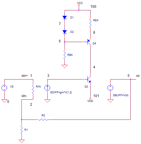
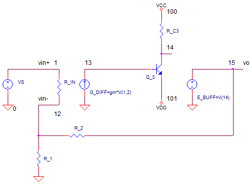
Let's compare the two load types - resistor and current source - each in their own small signal model. The small signal model greatly simplifies an audio amp into three stages: a differential amplifier (GDIFF), a voltage gain stage (Q3) and an output buffer (EBUFF). Feedback resistors R2 and R1 close the loop on the amplifiers for a gain of 10x.
The BJT current source (top of page) produces a constant current out of Q4 regardless of the voltage at it's collector. How can you set its output current? Set the Io through RE4.
Io ≈ VD1 / RE4.
where VD1=0.7V is a typical forward voltage of a diode. With RE4 = 650, the current is set to about 1.0 mA. (See BJT Constant Current Source. )
The gain stage with resistor has a couple of bragging rights - simplicity and low cost. This el cheapo design wins in the reduced parts count 1 to 5. But it performance may not be worth the cost savings.
SIGNAL GAIN
As a quick review, the differential stage converts the differential input voltage (vin+ - vin-) to a current (GDIFF). The gain stage (Q3) converts this current back to a voltage at V(4). How? Ic3 flows through through the resistance at Q3's collector developing a voltage.
V(4) = Ic3 * RC3.
What is RC3? For the resistor load, its simply the resistor RC3. For the active load, RC3 is the effective resistance created by the constant current source. And rumor has it - its quite high.
RESISTOR VS. ACTIVE LOAD
Which gain stage has the better performance? To compare them, we'll measure the gain from differential input voltage V(1,2) to collector voltage V(4), or GAIN = V(4)/V(1,2).
CIRCUIT INSIGHT Run an AC ANALYSIS ANALYSIS. In separate plot windows, plot the gains for the two amplifiers.
| Q3 Load | Gain from diff input to Q3 collector | |
| Resistor | V(14)/V(1,12) | |
| Current Source | V(4)/V(1,2) |
What did you see? The resistor performed well with a respectable gain of of 30,000 V/V. However, as you might have guessed, the active load knocked the gain out of the park with 1,200,000 V/V! Why? the effective resistance of a BJT collector - when wired as a constant current source - is typically very high.
HANDS-ON DESIGN Let's try to increase the gain of both circuits. Its fairly obvious how to increase the resistor load's gain. Try increasing resistor RC3 by a factor of 2 or 3. Rerun the simulation and check the gain. How much did it increase? Its should scale roughly with the resistor.
Now try increasing the effective resistance of the active load. How? Try decreasing RE4 by a factor of 2 or so (this will increase the output current). Rerun the simulation. Did the gain increase or decrease? Try increasing RE4 by a factor of 2 above the original 650. What happened to the gain?
OUTPUT DRIVE
A valid question is this: why not just increase resistor load RC3 until you get a huge gain like the current source? Sounds good. However, a major function of this stage is providing base current to drive the next stage - the output buffer. Typically, the next stage is an emitter follower requiring some base current drive.
Let's look at the resistor's drive capability. Suppose you've got an output signal of 10V with 15V supply. That means with RC3=15k you've only got (15V-10V)/15k=0.333mA to drive the next stage. Furthermore, you may need a lot more gain, so you increase RC3 to 300k. Unfortunately, the available drive just got cut to 0.033 mA.
On the other hand, the current source performs head and shoulders above the resistor by two bench marks: 1) It has a much higher gain, and 2) It provides a beefy 1.000mA drive throughout its voltage range, about -15 to 14 V.
SPICE FILE
Download the file or copy this netlist into a text file with the *.cir extension.
AMP_ACTIVE_LOAD.CIR
*
VS	1	0	AC	1 sin(0 0.1Vp 1kHz)

VCC	100	0	+15V
VDD	101	0	-15V


* AMPLIFIER WITH ACTIVE LOAD ***
* GAIN RESISTOR
R2	5	2	1000
R1	2	0	10

* DIFFERENTIAL STAGE
RIN	1	2	1E12
GDIFF 0 3   1 2  0.02

* GAIN WITH ACTIVE LOAD
*C	3	4	500PF
Q3	4 3 101 QNPN
*
* CURRENT SOURCE
D1	100	7	DNOM
D2	7	6	DNOM
RB4	6	0	5K
Q4 4 6 8 QMPSA56
RE4	8	100	650

* BUFFER
EBUFF	5 0 	4 0 1


* AMPLIFIER WITH RESISTOR LOAD ***
* GAIN RESISTOR
R_2	15	12	1000
R_1	12	0	10

* DIFFERENTIAL STAGE
R_IN	1	12	1E12
G_DIFF 0 13   1 12  0.02

* GAIN WITH RESISTOR LOAD
*C	13	14	500PF
Q_3	14 13 101 QNPN
*
R_C3	100	14	15000

* BUFFER
E_BUFF	15 0 	14 0 1


* MODELS
.MODEL QNPN NPN(   Bf=100 )
.MODEL DNOM D( )

.MODEL Qmpsa56 pnp
+IS=9.62586e-12 BF=246.647 NF=1.19008 VAF=19.1507
+IKF=0.332189 ISE=1.74278e-11 NE=1.95504 BR=0.1
+NR=1.49124 VAR=3.92539 IKR=4.71144 ISC=3.90265e-13
+NC=3.98982 RB=0.772559 IRB=0.184627 RBM=0.365314
+RE=0.00202964 RC=0.26419 XTB=0.467199 XTI=1
+EG=0.851752 CJE=4.05433e-11 VJE=0.4 MJE=0.748564
+TF=7.64992e-10 XTF=4.80943 VTF=12.6194 ITF=0.441135
+CJC=4.21506e-11 VJC=0.4 MJC=0.352218 XCJC=0.899996
+FC=0.180025 CJS=0 VJS=0.75 MJS=0.5
+TR=1e-07 PTF=0 KF=0 AF=1


* ANALYSIS
.AC DEC 5 10 100k
.PROBE
.END
© 2008 eCircuit Center