Output Stage
CIRCUIT
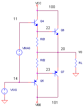
OUTPUT_STAGE.CIR Download the SPICE file
What makes a good output stage for an audio amplifier? Here are some desirables
1. Deliver large amounts of current into RL without self destructing.
2. Provide a high input impedance at the base of Q4, Q5.
3. Minimize distortion when transitioning between positive and negative output currents.
OUTPUT STAGE BASICS
Your basic output stage is the double emitter follower - a NPN pair (Q4, Q6) for positive output currents and a a PNP pair (Q5,Q7) for negative output currents. Also called a Darlington configuration, emitter followers have a gain of unity. The Darlington pair creates a super beta transistor. This means you can deliver a lot of amps to the outside world with small amounts of base current into Q4, Q5.
DELIVERING THE POWER
Here's a big job for a big transistor: deliver large currents without sending up smoke signals. These transistors, Q6 and Q7, need large die sizes to dissipate the heat as they pass beefy currents. This also means large packages to transfer the heat to PCBs and heatsinks. On the down side, big die sizes also mean large base capacitance that could slow down the output devices. (See distortion below)
HIGH INPUT Z
Unfortunately, high power transistors, Q6 and Q7, have low current gains (50 -100). This would require a lot of current from the previous stage. In other words, it presents a low impedance load to the previous stage, knocking down its precious voltage gain. So you can think of the drive devices, Q4 and Q5, as beta enhancers. These lower power drive transistors have current gains of 100 to 200 or more. Together they make up a Darlington configuration with a combined current gain of 2000+.
You can also think of emitter followers as load impedance multipliers. For example, for an 8 ohm load, the input resistance at Q4 looks like
Rin = RL · (β4 · β4)
= 8 · (100 · 200)
= 16,000 ohms
Way cool! 16k presents a much lighter load to the previous stage.
MINIMAL DISTORTION
The output stages has two unfortunate characteristics: cross-over distortion and switching distortion. Cross-over distortion happens because the drive signal must reach 2 x Vbe before the NPN pair turn on. Likewise, the drive signal must swing 2 x -Vbe to turn on the PNP pair. What happens to Vo while Vin is in the deadzone of 4 * Vbe? Vo just sits there at 0V. Our beautiful input sine wave gets hit with the ugly stick due to this cross-over distortion. What is the fix? A small bias voltage between Q4 and Q5, usually just a bit smaller than 4*Vbe, minimizes the deadzone.
What is switching distortion? Suppose Q6 is delivering a large positive current into RL. This power transistor also has a huge base capacitance that is charged up at this time. Now suppose, the output rapidly swings negative, requiring Q6 to turn off quickly and Q7 to turn on. Not so fast! The charge on the base capacitance needs to be pulled out of Q6 first. If Q6 does not turn off quickly enough, it may be still conducting when Q7 turns on! Bad situation. You may be allowing large destructive currents to flow while both Q6 and Q7 remain ON between the supply rails! Later we'll see how RE1 and RE2 may rescue this situation.
DRIVING AN 8 OHM LOAD
Let's run a SPICE simulation to see how this output stage operates. The voltage source VBIAS (initially set to 0V) will let you vary the drive bias to see its effect on cross-over distortion. (In a real audio amp, this bias is accomplished by diodes or a Vbe multiplier.) To test the stage we'll drive it with a 1 kHz sine wave.
VSIG 14 0 AC 1 SIN(-0.0V 10V 1KHZ)
To keep the output symmetrical, set the DC OFFSET of the sinewave (-0.0V initially) to negative half of the VBIAS voltage.
![]() CIRCUIT INSIGHT
Run a simulation of OUTPUT_STAGE.CIR. Plot the output
V(20) and the drive levels at V(11) and V(14). Because our VBIAS is
initially at 0V, you should see some major cross-over distortion. Notice how
Vo just sits at 0V while the input V(11) and V(14) travel through the dead
zone.
CIRCUIT INSIGHT
Run a simulation of OUTPUT_STAGE.CIR. Plot the output
V(20) and the drive levels at V(11) and V(14). Because our VBIAS is
initially at 0V, you should see some major cross-over distortion. Notice how
Vo just sits at 0V while the input V(11) and V(14) travel through the dead
zone.
HANDS-ON DESIGN Okay, let's try and minimize the dead zone. Set VBIAS to 1V. (Also set the SIN offset term to -0.5V for a symmetrical output.) Rerun the simulation. Nice! Notice how V(11) and V(14) are now separated. And most important, check out how the distortion of V(20) has been reduced. Keep increasing VBAIS until it appears the cross-over distortion is just about eliminated. How big is VBIAS at this point?
OUTPUT CURRENT, INPUT Z AND POWER
CIRCUIT INSIGHT How much current is delivered to the load? Set VBIAS to 2V and the sine offset to -1V. Open a new plot window and plot the output currents IC(Q6) and IC(Q7). You should see a peak current of approximately Ic7 = 10V / 8 = 1.2 A. Check out how each NPN or PNP pair takes turns conducting on alternating half cycles.
Now check out the peak current in the drivers by plotting IC(Q4) and IC(Q6). You can calculate the current gain through the output drivers Ic6 / Ic4. It's probably less than 100 or so.
How much base current is required at the drivers? Open a new plot window and plot these currents IB(Q4) and IC(Q5). What is the equivalent input resistance at Q4's base? You can estimate it from the drive signal and the base current: Rin = Vb4 / Ib4 = 10V / 40 u = 25k ohm. A bigger Rin means less loading on the previous stage.
Finally, how much power is dissipated in Q6 and Q7? The instantaneous powers are easily plotted as IC(Q6)*V(100,20) and IC(Q7)*V(101,20). How do you calculate the average power? PSPICE comes with an AVG() function. (Most simulators have some averaging function.) Plot the average power in Q6 with
AVG( IC(Q6)*V(100,20) )
Why is this useful? The average power helps predict the temperature rise in the transistor. This key insight helps you pick a heatsink to avoid destroying your output devices!
SWITCHING DISTORTION
To investigate switching distortion, let's crank up the frequency to 10 kHz. Change the signal and the transient command.
VSIG 14 0 AC 1 SIN(-0.0V 10V 10KHZ)
.TRAN 0.5US 0.2MS 0US 1US
CIRCUIT INSIGHT Rerun the SPICE analysis and plot the output currents IC(Q6) and IC(Q7). What's happening? Oh the horror! Both transistors Q6 and Q7 conduct at the same time. As you can see, Ic6 does not go to zero when its half cycle is complete. Why? As mentioned before, the large base capacitance of Q6 is not fully discharged at the time Q7 starts conducting. The ill effects of this are output distortion and excessive power dissipated in the Q6 and Q7.
HANDS-ON DESIGN Okay, let's try and minimize the switching distortion. We need a way to remove the base charge of Q6 and Q7. This is where RE1 and RE2 enter the scene. Maybe they can provide a discharge path for the base capacitances. Initially RE1 = RE2 = 50k which has little effect on the circuit. But try reducing their value to 5k and below. Rerun the simulation. At what point does the Q6 and Q7 start to turn off quicker? What value of RE1 and RE2 makes the output transistors turn off cleanly at the end of their half cycle?
SPICE FILE
Download the file or copy this netlist into a text file with the *.cir extension.
OUTPUT_STAGE.CIR - DARLINGTON OUTPUT WITH VOLTAGE BIAS
*
*
* POWER SUPPLIES
VCC	100	0	DC	+15V
VEE	101	0	DC	-15V
*
VBIAS	11	14	DC	0.0
VSIG	14	0	AC 1	SIN(-0.0V 10V 1KHZ)

*
* OUTPUT STAGE
Q4	100 11	22	Q2N3904
Q6	100 22	20	QTIP31
Q5	101 14	23	Q2N3906
Q7	101 23	20	QTIP32
RE1	22	20	500
RE2	23	20	500
*
* LOAD
RL	20	0	8
*
*
* DEVICE MODELS
.model Q2N3904	NPN(Is=100.9f Xti=3 Eg=1.11 Vaf=115.7 Bf=278 Ne=1.894
+		Ise=14.35p Ikf=.1594 Xtb=1.5 Br=.118 Nc=2 Isc=0 Ikr=0 Rc=.6
+		Cjc=4.929p Vjc=.75 Mjc=.3333 Fc=.5 Cje=7.707p Vje=.75
+		Mje=.3333 Tr=290.3n Tf=296.5p Itf=.2 Vtf=10 Xtf=2 Rb=10)

.model Q2N3906	PNP(Is=1.434f Xti=3 Eg=1.11 Vaf=30.7 Bf=234.1 Ne=1.293
+		Ise=1.434f Ikf=.1784 Xtb=1.5 Br=3.515 Nc=2 Isc=0 Ikr=0 Rc=1.5
+		Cjc=6.901p Vjc=.75 Mjc=.3333 Fc=.5 Cje=7.114p Vje=.75
+		Mje=.3333 Tr=27.74n Tf=306.3p Itf=.1 Vtf=10 Xtf=20 Rb=10)

.MODEL Qtip31 npn
+	IS=1e-09 BF=3656.16 NF=1.23899 VAF=10
+	IKF=0.0333653 ISE=1e-08 NE=2.29374 BR=0.1
+	NR=1.5 VAR=100 IKR=0.333653 ISC=1e-08
+	NC=1.75728 RB=6.15083 IRB=100 RBM=0.00113049
+	RE=0.0001 RC=0.0491489 XTB=50 XTI=1
+	EG=1.05 CJE=3.26475e-10 VJE=0.446174 MJE=0.464221
+	TF=2.06218e-09 XTF=15.0842 VTF=25.7317 ITF=0.001
+	CJC=3.07593e-10 VJC=0.775484 MJC=0.476498 XCJC=0.750493
+	FC=0.796407 CJS=0 VJS=0.75 MJS=0.5
+	TR=9.57121e-06 PTF=0 KF=0 AF=1

.MODEL Qtip32 pnp
+	IS=1e-09 BF=134.366 NF=1.29961 VAF=10
+	IKF=0.742988 ISE=1e-16 NE=1.40014 BR=0.1
+	NR=1.46599 VAR=100 IKR=3.21978 ISC=1e-16
+	NC=2.71657 RB=7.44433 IRB=2.41268 RBM=0.218936
+	RE=0.0152284 RC=0.0761421 XTB=0.1 XTI=1
+	EG=1.05 CJE=3.26474e-10 VJE=0.446178 MJE=0.464223
+	TF=1e-08 XTF=3.50642 VTF=8.2848 ITF=0.0305862
+	CJC=3.07595e-10 VJC=0.77548 MJC=0.476497 XCJC=0.799334
+	FC=0.8 CJS=0 VJS=0.75 MJS=0.5
+	TR=9.57121e-06 PTF=0 KF=0 AF=1

.TRAN	5US 2MS 0US 10US
*.TRAN	0.5US 0.2MS 0US 1US

.PROBE
.END
© 2007 eCircuit Center