FUNCTION GENERATOR - PART
2
Sine-Wave Generator
CIRCUIT
FUNCTION_GENERATOR.CR Download the SPICE file
In Part 1, we learned how to take a collection of ordinary parts and transform them into a circuit that generates a triangle or square wave output! But where does the sine wave come from? This topic shows you how to take the triangle wave waveform and bend it into a sine wave.
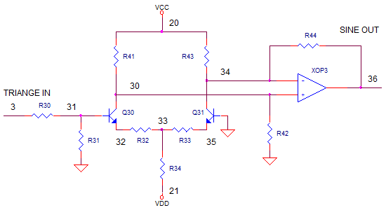
SINE SHAPER
What type of circuit is needed? A simple circuit with a non-linear response, such as a transistor differential amplifier, can serve us well.
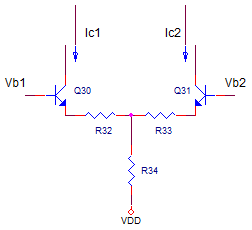
► For small differntial inputs Vin = Vb1-Vb2 across the bases,
the differential output current Io = Ic1-Ic2 is linear.► For large Vin, the gain (gm=Io/Vin) is gradually reduced resembling soft clipping.
To help adjust its transfer function, resistors R32 and R33 are added. Increasing or decreasing these resistors causes the response to be more or less linear.
CURRENT TO VOLTAGE TRANSLATOR
How do we take our differential output current from the the Q1, Q2 pair above and convert it back to voltage? Here's a handy circuit that's easier to analyze than it looks. The transistor outputs are modeled as current sources. Although the transistors do have an output impedance across current sources, the value is typically so high where it won't significantly affect circuit operation.
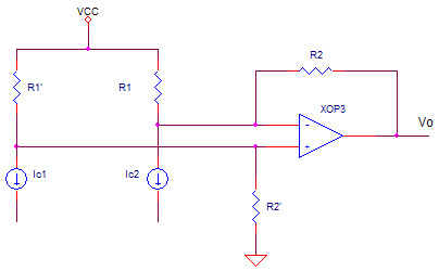
Let's apply superposition for all three signal sources Vcc, Ic1 and Ic2. Assume R2/R1=R2'/R1'.
1. Find Vo due to Ic1 with Ic2 OFF (Open circuit) and Vcc OFF (Short to GND).
Ic1 flows into the parallel combo of R1 and R2 to create a voltage, then gets multiplied by the non-inverting gain.Vo1 = Ic1 * R1'||R2' * (R2+R2)/R1
= Ic1 * R1'*R2'/(R2'+R1') * (R2+R2)/R1
= Ic1 * R22. Find Vo due to Ic2 with Ic1 OFF (Open circuit) and Vcc OFF (Short to GND).
Ic2 flows into feedback resistor R2 creating a voltage much like a transimpedance amplifier.Vo2 = -Ic2 * R2
3. Find Vo due to Vcc with Ic1 and Ic2 OFF (Open circuit).
Removing Ic1 and Ic2 leaves us with a differential amplifier. Because Vcc is applied to both inputs, the output is equal to 0V.Vo3 = (Vcc - Vcc) * R2/R1 = 0V
4. Adding all three outputs together you get
Vo = Vo1 + Vo2 + Vo3
= Ic1*R2 - Ic2*R2 + 0
= (Ic1 - Ic2)*R2
The circuit nicely converts the current difference into a voltage scaled by R2!
SIMULATION
Let's see how this circuit works. Notice R30 and R31 attenuate the signal by ~10x so that the differential pair is not over driven with too large of an input. Choosing R34=5k sets up about 0.5mA flowing in each transistor. The resistors for the current to voltage converter were initially chosen as R41,42,43,43=2k. You can increase R42 and R44 to increase the output.
CIRCUIT INSIGHT Run a transient simulation and plot the triangle wave output V(3). In another plot window, add the transistor collector currents IC(Q30) and IC(Q31). Finally go back to the original plot and add the sine wave output at V(36) to see the difference of currents converted back to a voltage. In many classic function generator circuits, this is how the triangle wave becomes a sine wave!
SINE ADJUST
HANDS-ON DESIGN Now, let's monkey with the controls. Reduce linearizing resistors R32,33 from 120 to just 12 ohms. Rerun the simulation and check out V(36). What happened to the beautiful sine wave. Looks like there's too much clipping! Try increasing R32,33 to 240 ohms. What happened to the output V(36). Looks like the gain is too linear where the output starts resembling the triangle wave.
You can also adjust the non-linearity by adjusting the input attenuator. Set R32,33 to 12 ohms and reduce R31 until you get a better looking sine wave.
Finally, you can scale the output by adjusting R42,44. Try increasing or decreasing R42,44 by a factor of 2. Rerun the simulation. Did the output scaled as you expected?
SPICE FILE
Download the file or copy this netlist into a text file with the *.cir extension.
FUNCTION_GEN.CIR - TRIANGLE, SQUARE, SINE GENERATOR
*
* FREQUENCY CONTROL
VS	1	0	1VDC
*VS	1	0	SIN(1V	0.4VP	100HZ)
* INVERTER
R3	1	4	10K
R4	4	5	10K
XOP2	0 4 5	OPAMP1

* INTEGRATOR
R1	1	2	10K
R2	6	2	5K
S1	6 5  15 0 SWA
CI	2	3	10NF IC=0V
XOP1	0 2 3	OPAMP1
*
* THRESHOLDS
RTH1 20 22  5K
RTH2 22 0  5K
RTH3 0 23  5K
RTH4 23 21  5K
*
* COMPARATORS
XCMP1	3 22 11 COMP1
XCMP2	23 3 12 COMP1
*
* RS FLIP-FLOP
XNOT1	11 13 20 NOT
XNOT2	12 16 20 NOT
XNAND1	13 14 15 20	NAND
XNAND2	15 16 14 20	NAND

* PWR FOR LOGIC GATES AND THRESHOLDS
VCC	20	0	+5V
VDD	21	0	-5V

* SINE SHAPER - DIFF AMP
R30	3	31	10K
R31	31	0	1K
*
Q30	30 31 32	QNPN
Q31	34 0  35 QNPN
R32	32	33	120
R33	35	33	120
R34	33	21	5K
* CURRENT TO VOLTAGE AND LEVEL SHIFTER
R41	20	30	2K
R42	30	0	2.5K
R43	20	34	2K
R44	34	36	2.5K
XOP3	30 34 36	OPAMP1
*
* SUBCIRCUITS AND MODELS ***********************************
*
.SUBCKT NAND 1 2 3 4
* TERMINALS A B OUT VCC
RL	3	4	500
CL	3	0	10PF
S1	3 5	1 0 	SW
S2	5 0	2 0 	SW
.ENDS
*
.SUBCKT NOT 1 3 4
* TERMINALS A OUT VCC
RL	3	4	500
CL	3	0	10PF
S1	3 0	1 0 	SW
.ENDS
*
.SUBCKT COMP1  1 2 5
* TERMINALS: 1-INPUT+, 2-INPUT-, 5-OUTPUT
* DIFF AMP WITH HYSTERESIS
EDIFF	3	0	VALUE = { V(1) - V(2) +  V(5)/1000}
* FREQUENCY RESPONSE
RP1	3	4	500
CP1	4	0	100PF
* LIMITER
EOUT	5	0	TABLE {V(4)} = (-5MV 0V) (5MV, 5V)
.ENDS
*
*
* OPAMP MACRO MODEL, SINGLE-POLE WITH 15V OUTPUT CLAMP
* connections:      non-inverting input
*                   |   inverting input
*                   |   |   output
*                   |   |   |
.SUBCKT OPAMP1	    1   2   6
* INPUT IMPEDANCE
RIN	1	2	10MEG
* DC GAIN=100K AND POLE1=100HZ
* UNITY GAIN = DCGAIN X POLE1 = 10MHZ
EGAIN	3 0	1 2	100K
RP1	3	4	100K
CP1	4	0	0.0159UF
* OUTPUT BUFFER AND RESISTANCE
EBUFFER	5 0	4 0	1
ROUT	5	6	10
.ENDS
*
*
.MODEL	SWA	VSWITCH(VON=2 VOFF=3 RON=1 ROFF=1e6)
.MODEL	SW	VSWITCH(VON=3 VOFF=2 RON=10 ROFF=100K)
.model	QNPN	NPN(BF=100)
*
*
* ANALYSIS *************************************************
.TRAN 	1US  2MS UIC
.IC V(15)=0 V(14)=5
*
.PROBE
.END
© 2009 eCircuit Center