FUNCTION GENERATOR - PART
1
Triangle and Square-Wave Generator
CIRCUIT
FUNCTION_GENERATOR.CR Download the SPICE file
At some time, you've probably run into this magical instrument in the lab - the function generator. Just turn the waveform selector knob and a triangle, square or sine wave appears at the output! Turn another knob and the frequency of the signal changes. Now you can feed the square wave into an amplifier you're testing to see how quickly it responds. Is there any over shoot or ringing? Or maybe you're testing an audio amplifier and you feed it a 1 kHz sine wave. Is there any distortion at the output? I looked at my handy function generator and wondered what kind of circuit creates these waveforms? A search on the web produced a few schematics. Although they all took different circuit approaches, the essence of each one resembled the overall topology shown above.
TRIANGLE WAVE
At the core of the function generator is a triangle wave generator. How do you generate a triangle wave? The most common way is to get a capacitor and then alternate charging it and discharging it. But how to you get a nice linear ramp across the capacitor? The key here is to charge and discharge it with a constant current source. Mathematically, here's how it works. A capacitor integrates a current, i.
vo = 1/C · ∫ i dt
By making the current constant I, you can take it outside the integral.
vo = 1/C · I ∫ dt
= 1/C · I · ∆t
= ( I · ∆t ) / C
What your left with is a simple equation for voltage that's a linear function of the time interval ∆t.
CONSTANT CURRENT INTEGRATOR
Looking at function generator schematics you'll find different ways to implement constant current sources and integrators. One circuit uses the classic op amp integrator. To create the negative ramp, the circuit looks like this.
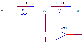
The key here is that the op amp keeps its negative input at 0V. This makes writing the equations a snap. For the negative going ramp, the currents are
I1 = vs / R
Ic = I1
Essentially, vs and R force a constant current I1 through the resistor. This same current flows through C. The output voltage becomes
vo = -vc
= -Ic · ∆t / C
= -I1 · ∆t / C
= - vs / R · ∆t / C
To create a positive going ramp, an additional resistor is switched in. This creates a current of opposite polarity flowing through C.
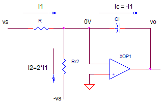
For the positive going ramp, the currents are
I1 = vs / R
I2 = -vs / R/2 = -2·vs / R = -2·I1Ic = I1 + I2
= I1 - 2·I1
= -I1
By switching in R2, a current of -I1 is forced through C. The output voltage becomes
vo = -vc
= -Ic · ∆t / C
= -(-I1) · ∆t / C
= +I1 · ∆t / C
= + vs / R · ∆t / C
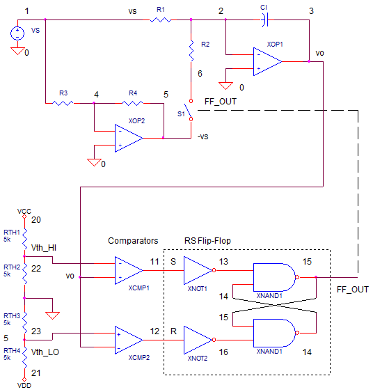
In the SPICE circuit, vs and R1=10k set up I1. An inverter XOP2 creates -vs from vs. I2 is created using voltage -vs and with R2=5k. R2 is switched into the circuit by voltage-controlled switch S1. The integrator is created by XOP1 and CI.
RAMP BOUNDARIES
The next challenge is
switching between the positive and negative ramps. Typically, two voltage thresholds
(high and low) are created to set the boundaries of the ramp
voltages. RTH1 and RTH2 set the positive threshold Vth_HI=+2.5V, while RTH3 and RTH3 set
the negative threshold
Vth_LO=-2.5V.
Comparator XCMP1 compares the ramp voltage to Vth_HI. XCMP1's output goes from LO to HI when vo reaches Vth_HI=+2.5V. Likewise, XCMP2's output goes from LO to HI to high when vo reaches to Vth_LO=-2.5V.
The outputs of XCMP1 and XCMP2 are fed to the Set and Reset input of the flip-flop. Positive edges at the Set and Reset inputs will set the flip-flop output HI or LO, respectively.
SET / RESET FLIP FLOP
Why use the SR flip-flop? The Flip-Flop's output serves as the square wave output. It also controls the S1. The state of of S1 (ON or OFF) determines if op amp XOP1 is generating a positive or negative ramp.
Although the RS Flip-Flop can be modeled in many ways, the classic cross-coupled NAND gate defines this function. Furthermore, the NANDs were created from simple switches so running the SPICE file does not require a mixed-mode (analog / digital) simulator.
THE BIG PICTURE
Here are the key actions of the function generator. During the positive ramp:
- vo ramps POS
- vo reaches Vth_HI
- XCMP1 generates POS output to SET input of flip-flop
- Flip-flop output goes HI turning OFF S1
- vo starts going NEG.
During the negative ramp:
- vo ramps NEG
- vo reaches Vth_LO
- XCMP2 generates POS output to RESET input of flip-flop
- Flip-flop output goes LO turning ON S1
- vo starts going POS.
SIMULATION
Let's design a function generator and take it out for a spin. Suppose you are asked to generate a 1 kHz triangle wave (To=1.0 ms). Initially set VS=1V, R=10k, R2=5k, Vth_HI=+2.5V, Vth_LO=-2.5V. The thresholds imply that the negative ramp will change by
∆vo = Vth_LO - Vth_HI = -5V
Now the big question is this: what C do we need such that vo will change -5V in ∆t = To/2 = 0.5 ms? Starting with ∆vo = vs / R · ∆t / C we solve for C.
C = -vs / R · ∆t / ∆vo
= -1V / 10k *0.5ms / -5V
= 10 nF
CIRCUIT INSIGHT Run a transient simulation and plot the output V(3). Does the output ramp linearly up and down between the thresholds +2.5V and -2.5V? Way cool! I still get a kick out of seeing signal generators do their thing.
In the same window, plot the comparator's outputs V(11) and V(12). You can see the outputs flip state as the ramp exceeds the upper or lower threshold. However, the ramp quickly direction and the comparator output changes state, leaving only a narrow pulse.
Open a new plot window and add the SR flip-flop output V(15). This is
the square wave output!
V(15)
should go HI at the leading edge of XCMP1 output V(11) and go LO at the
leading edge of XCMP2 output V(12).
The flip-flop's output V(15) controls the state of the switch S1. When V(15) goes LO, S1 turns ON creating a POS ramp. When V(15) goes HI, S1 turns OFF creating a NEG ramp.
TURN THE DIALS
Okay let's play with some component values and see what happens.
HANDS-ON DESIGN Here's a few things to try.
- Try changing vs to 2x or 1/2x of its value. This will increase the constant current. What will happen to the frequency?
- Change threshold resistors RTH2 and RTH3 to increase the thresholds. The triangle wave has further to travel. What will this do to the operating frequency?
- Try changing CI by 10x or 0.1x of its value. Will this create a faster or slower ramp? This is how generators can change the frequency range by a decade at a time.
- Change the values of R1 and R2 Hoe does this effect the rate of change at vo?
- What about modulating the output? Comment out (place a "*" at the beginning of a line) the VS statement with the DC value. Enable the VS statement with the SIN statement (delete the "*"). Extend the simulation to 20 ms and see how a sine wave at VS effects the operating frequency.
ACCURACY
CIRCUIT INSIGHT For all our brilliant insight and calculations, the period of operation seems a tad too long. Why? There's a bit of a time lag in the comparator. The voltage ramp must exceed the threshold by a finite amount for the comparator to switch. Then there's another lag through the RS flip-flop and the time it takes S1 to change states. At low frequencies, you may not notice either of these effects. However, the higher in frequency you go, the greater the error. To compensate for this, adjust VS to fine tune the frequency.
Change CI to 1nF or 0.1nF and change the simulation length to 0.2 ms or 0.02ms. Run a simulation and plot V(3). How accurate is the period? Look at the comparator outputs V(11) and V(12). Notice how their output pulse width gets large compared to the period as frequency increases. Can you tweak VS for a precise 10kHz or 100kHz triangle wave.
SPICE MODELS
CIRCUIT INSIGHT Notice, the NAND and NOT gates include a small capacitor to delay the output slightly. Without this, SPICE would freeze up as it tried to calculate the transient solution. Need proof? Remove the capacitors in the subcircuits by placing an "*" before the CL statements. Run a simulation and watch what happens.
CIRCUIT INSIGHT Three sections make this simple comparator: differential input, low-pass filter and output limiting. EDIFF implements the differential comparison and hysteresis functions.
EDIFF 3 0 VALUE = { V(1) - V(2) + V(5)/500 }
Hysteresis helps the comparator output switch quickly, even with slow moving inputs. As you can see, it feeds a fraction of the output V(5) to the input helping it swing faster through the threshold. Low-pass filter, RP1 and CP1, adds delay to the device. Without it, SPICE may sputter and grind to a halt when calculating the transient response. Lastly, the TABLE function creates the output limiter: V(4) = 5V for inputs > 1 mV; V(4) = 0V for inputs < -1 mV. For inputs between -1 mV and +1 mV, V(4) is a linear function between the points defined by the table.
ROUND UP
Hey, that was a lot of ideas to absorb in a single page. And we haven't even touched the sin wave generator section! Take heart - it took me some time to research, play with and digest the circuits and theory. But that's part of the fun. Part 2 will take our linear ramp and bend it into something that resembles a sine wave.
SPICE FILE
Download the file or copy this netlist into a text file with the *.cir extension.
FUNCTION_GEN.CIR - TRIANGLE, SQUARE, SINE GENERATOR
*
* FREQUENCY CONTROL
VS	1	0	1VDC
*VS	1	0	SIN(1V	0.4VP	100HZ)
* INVERTER
R3	1	4	10K
R4	4	5	10K
XOP2	0 4 5	OPAMP1

* INTEGRATOR
R1	1	2	10K
R2	6	2	5K
S1	6 5  15 0 SWA
CI	2	3	10NF IC=0V
XOP1	0 2 3	OPAMP1
*
* THRESHOLDS
RTH1 20 22  5K
RTH2 22 0  5K
RTH3 0 23  5K
RTH4 23 21  5K
*
* COMPARATORS
XCMP1	3 22 11 COMP1
XCMP2	23 3 12 COMP1
*
* RS FLIP-FLOP
XNOT1	11 13 20 NOT
XNOT2	12 16 20 NOT
XNAND1	13 14 15 20	NAND
XNAND2	15 16 14 20	NAND

* PWR FOR LOGIC GATES AND THRESHOLDS
VCC	20	0	+5V
VDD	21	0	-5V

* SINE SHAPER - DIFF AMP
R30	3	31	10K
R31	31	0	1K
*
Q30	30 31 32	QNPN
Q31	34 0  35 QNPN
R32	32	33	120
R33	35	33	120
R34	33	21	5K
* CURRENT TO VOLTAGE AND LEVEL SHIFTER
R41	20	30	2K
R42	30	0	2.5K
R43	20	34	2K
R44	34	36	2.5K
XOP3	30 34 36	OPAMP1
*
* SUBCIRCUITS AND MODELS ***********************************
*
.SUBCKT NAND 1 2 3 4
* TERMINALS A B OUT VCC
RL	3	4	500
CL	3	0	10PF
S1	3 5	1 0 	SW
S2	5 0	2 0 	SW
.ENDS
*
.SUBCKT NOT 1 3 4
* TERMINALS A OUT VCC
RL	3	4	500
CL	3	0	10PF
S1	3 0	1 0 	SW
.ENDS
*
.SUBCKT COMP1  1 2 5
* TERMINALS: 1-INPUT+, 2-INPUT-, 5-OUTPUT
* DIFF AMP WITH HYSTERESIS
EDIFF	3	0	VALUE = { V(1) - V(2) +  V(5)/1000}
* FREQUENCY RESPONSE
RP1	3	4	500
CP1	4	0	100PF
* LIMITER
EOUT	5	0	TABLE {V(4)} = (-5MV 0V) (5MV, 5V)
.ENDS
*
*
* OPAMP MACRO MODEL, SINGLE-POLE WITH 15V OUTPUT CLAMP
* connections:      non-inverting input
*                   |   inverting input
*                   |   |   output
*                   |   |   |
.SUBCKT OPAMP1	    1   2   6
* INPUT IMPEDANCE
RIN	1	2	10MEG
* DC GAIN=100K AND POLE1=100HZ
* UNITY GAIN = DCGAIN X POLE1 = 10MHZ
EGAIN	3 0	1 2	100K
RP1	3	4	100K
CP1	4	0	0.0159UF
* OUTPUT BUFFER AND RESISTANCE
EBUFFER	5 0	4 0	1
ROUT	5	6	10
.ENDS
*
*
.MODEL	SWA	VSWITCH(VON=2 VOFF=3 RON=1 ROFF=1e6)
.MODEL	SW	VSWITCH(VON=3 VOFF=2 RON=10 ROFF=100K)
.model	QNPN	NPN(BF=100)
*
*
* ANALYSIS *************************************************
.TRAN 	1US  2MS
*
.PROBE
.END
© 2009 eCircuit Center