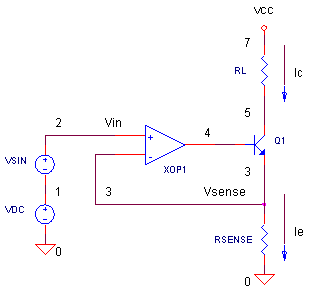
Current Source with Floating Load
CIRCUIT
CURR_SRC1.CIR Download the SPICE file
Getting optimum performance in certain applications requires that some components - sensors, DC motors, transistors - be driven or biased by a constant current. We're mostly familiar with voltage regulators and their ability to maintain a constant voltage under varying current conditions. In this application, your challenge is to provide a constant current regardless of the voltage developed across the load. However, there are errors and voltage limitations to be reckoned with. But once you understand a few simple principles of this circuit, you can avoid the troubled waters.
HOW IT WORKS
The circuit above maintains a current through a floating load RL (neither end is connected to ground.) The key to the circuit's operation is in placing a current sensing resistor RSENSE in the op amp feedback loop. The current delivered to the load RL is
I = Vin / RSENSE
How does the circuit work? Three simple functions help this circuit accomplish its goal. (Remember, no current flows into the op amp's input terminals.)
-
The op amp automatically adjusts its output (Q1's base drive) to bring its negative input equal to the positive input. This means that Vsense = Vin.
-
A simple application of Ohms law now tells you the current in RSENSE; I = VRSENSE / RSENSE.
-
Q1 delivers the current. And because Q1's currents are related by Ic ≈ Ie, the same current that is developed through RSENSE must also flow through RL.
CURRENT SOURCE
CIRCUIT INSIGHT Run a simulation of CURR_SRC1.CIR. The input V(2) is actually made up of two sources: VDC and VSIN. For now, we'll drive the input with a DC voltage only (VSIN is set to 0V). Plot the input voltage V(2), the voltage across RSENSE V(3) and the voltage across the load V(7,5). If the op amp is doing its job, then V(3) = V(2) = 1V. Now, you can easily calculate the current in RSENSE as I = 1V / 10 Ω = 100mA. What's the current in the load RL = 100 Ω? From the measured output voltage, the current is calculated as
I = V(7,5) / RL ≈ 10V / 100 Ω = 100mA
The circuit has delivered the goods to RL as advertised! Now take a look at the op amp's output voltage V(4). What is its level in order to achieve VSENSE =1 V?
HANDS-ON DESIGN Pick a new value for the load resistor RL, say 10 or 50 Ω. Rerun the simulation. Is 100mA is still being delivered to the load? Now suppose you want to change the constant current to a lower value. To accomplish this, you have two choices. You can either lower the input voltage VIN or increase RSENSE. Choose a different value for the constant current. Then make changes to the circuit to accomplish the goal. (Example: For I = 10 mA, either lower VDC to 0.1V or increase RSENSE to 100 Ω. ) Test drive the new circuit. Is the output current what you expected?.
VOLTAGE LIMITS
Depending on the circuit, a current source has a certain compliance. This is simply the output voltage range over which the current can be delivered accurately. What is the biggest limiting factor in the compliance? The VCC power supply of course. You can't develop a bigger voltage than VCC across the load. If you need to, you might have to increase VCC. What else eats into voltage available for the load? As you can see, both VRSENSE and VCE are in series with the load. This will influence your choice of RSENSE. You want it big enough to convert the current into a healthy voltage signal VSENSE. On the other hand, you don't want it too big where it cuts into your compliance range.
HANDS-ON DESIGN Run a few simulations with VDC = 1 V and RSENSE = 10 Ω. Increase RL to values like 100, 125, 150 Ω and check the output current I = V(7,5) / RSENSE. What's the largest value of RL before we hit our head into compliance range. For RL = 200 Ω, how much do you have to jack up VCC to make 100 mA happen with this load?
CURRENT ERRORS
How accurate is the current generated in RL? Run a simulation with VDC=1 V, RSENSE = 10 Ω and RL = 100 Ω. Open a separate plot window and display the currents in RSENSE and RL by adding traces I(RSENSE) and I(RL). What's going on here? Although I(RSENSE) is equal to our expected 100 mA, I(RL) is only at 99 mA! Where did the other 1 mA go? Turns out that the equation above relating Q1's currents, Ie ≈ Ic, can be more accurately written as Ie = Ic + Ib. And because Ie = IRSENSE and Ic = IRL, you can calculate the current error as
IRSENSE = Ie; IRL = Ic = Ie - Ib
Ierror = IRSENSE - IRL
= Ib
= Ic / β
The error really boils down to the base current! Need to reduce error - reduce Ib. Also note, the error is inversely related to the current gain β. To verify this, remember the target current is 100 mA and β = 100. Therefore, we calculate the error as 100 mA / 100 = 1 mA which agrees with our measured error!
HANDS-ON DESIGN Reduce the error in your circuit by selecting a transistor with a higher current like β = 150 or 200. You can change β in Q1 by modifying the BF parameter in the transistor model statement.
.model QNOM NPN(BF=100)
(In any model statement, the unlisted parameters are set to their default values.) Run a new simulation. Does your calculated error Ic / β match your simulated one? How else can you reduce error? By using output devices with even smaller or negligible drive currents (Darlington transistors, JFETS, MOSFETS), you can tighten up the accuracy further.
WILD AND WOOLY WAVEFORMS
What happens to the output voltage waveforms when you drive the input with a sinewave and place reactive components in load? Throw some AC drive (0.6 V peak sinewave) on top of the DC input by modifying VSIN to look like
VSIN 2 1 SIN(0VOFF 0.6VPEAK 1KHZ)
Then place a capacitor like 5 uF or so across RL by adding the statement CL 7 5 5UF. Test drive the circuit and plot the "current" V(3) and the output voltage V(7,5). Recalling the nature of capacitive reactance, you should see the current V(3) leading the voltage V(7,5). Want to see the voltage lead the current? Replace the parallel RC at the load with a series RL.
FURTHER ADVENTURES
Another factor influencing the accuracy of output current is RSENSE. Change RSENSE by a few percent and what happens? The output current changes by the a few percent. Why? Because the sensing element in a feedback loop is one of the most critical components. Its your measure of output current. If RSENSE has a tolerance of +/-5%, the output current will have the same error.
You may have noticed that this circuit is a unidirectional current source - current flows in one direction only. Need current to flow in the opposite direction? Just change Q1 to an PNP device and invert the polarity of VDC and VCC.
SIMULATION NOTE
The op amp is modeled using a subcircuit named OPAMP1. Although the guts of an op amp can contain 20 transistors or more, this model mimics only the higher level (or macro) functions of the device. The result is a simple model requiring only a handful of components. For a more detailed look inside, see the Basic Op Amp Model.
Subcircuits are handy ways of inserting a particular circuit into one or more places of the main circuit. They're easy to define and use. Check them out in Why Use Subcircuits?
SPICE FILE
Download the file or copy this netlist into a text file with the *.cir extention.
CURR_SRC1.CIR - OPAMP CURRENT SOURCE, FLOATING LOAD
*
* INPUT VOLTAGE (DC + SINEWAVE)
VIN	1	0	DC	1V
VSIN	2	1	SIN(0VOFF 0VPEAK 1KHZ)
*
* OPAMP
XOP1	2 3	4	OPAMP1
Q1	5 4	3	QNOM
RSENSE 3	0	10
VCC	7	0	DC	15V
*
* LOAD
RL	7	5	100
*
*CL	7	5	5UF
*RS	7	6	10
*LS	6	5	10MH
*
.model	QNOM	NPN(BF=100)
*
* OPAMP MACRO MODEL, SINGLE-POLE
* connections:      non-inverting input
*                   |   inverting input
*                   |   |   output
*                   |   |   |
.SUBCKT OPAMP1      1   2   6
* INPUT IMPEDANCE
RIN	1	2	10MEG
* GAIN BANDWIDTH PRODUCT = 10MHZ
* DC GAIN (100K) AND POLE 1 (100HZ)
EGAIN	3 0	1 2	100K
RP1	3	4	1K
CP1	4	0	1.5915UF
* OUTPUT BUFFER AND RESISTANCE
EBUFFER	5 0	4 0	1
ROUT	5	6	10
.ENDS
*
* ANALYSIS
.TRAN	0.01MS 2MS
*
* VIEW RESULTS
.PRINT TRAN	V(2) V(7,5)
*.PRINT	TRAN I(RSENSE) I(RL)
.PROBE
.END
© 2002 eCircuit Center