Part 3
Band Cut / Boost - Series LCR and Pot
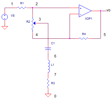
CIRCUIT
OP_CUT_BOOST_LCR_POT.CIR Download the SPICE file
This topic continues a four part series in the design of a graphic equalizer circuit.
1. Band Cut and Boost - Series LCR
2. Cut/Boost - Single Pot
3. Band Cut/Boost - Series LCR and Pot.
4. Simulated Inductor and Graphic EQ Circuit
Part 3 of the Graphic Equalizer Series combines the LCR Filter and the pot. In Part 1, the cut and boost functions were accomplished with two separate circuits. Part 2 showed the cut and boost function in a single circuit. Part 3 combines Parts 1 and Part 2 to achieve a single circuit that can cut or boost a band of frequencies depending on the position of the potentiometer's wiper.
OUTSIDE THE BAND
Far away from the series LCR's center frequency fo, the high
impedance of the LCR leg looks like an open to the remainder of the circuit.
You're left with the following circuit.
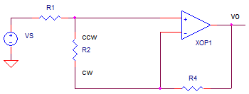
At first this circuit appears a bit strange, I had never seen this configuration. But recalling some basics, you can assume the op amp's inputs (Vpos and Vneg) are held at the same potential. This implies no current through R2 (and therefore no current in R1 or R4) The upshot of all this is that Vpos = VS and Vneg = Vpos and finally Vo=Vneg=VS. More simply stated, this circuit behaves as a unity gain buffer!
The bottom line: outside the frequency band of interest, the circuit passes the signal with no cut or boost, regardless of the wiper's position.
INSIDE THE BAND
At the center frequency fo, the high impedance of the LCR leg looks
R3 only! Why? Because ZL and ZC are equal and opposite and there fore cancel
each other leaving only R3.
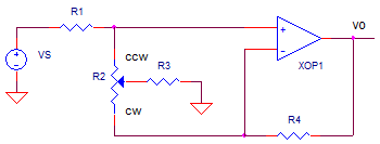
This circuit should ring a bell. We discovered it's operation in Part 2 where the extreme wiper positions Fully CCW and fully CW gave a cut or boost to the signal, respectively. At the center position, as you might have guessed passes the the signal at unity gain - no cut or boost.
The bottom line: inside the frequency band of interest, the circuit
boots or cuts the signal, depending on the wiper's position.
SPICE TEST
In Part 1, the LCR leg was designed for boost or cut of a about K=10x
centered around 800 Hz with a Q of 1.7. To test the EQ circuit, set RPOS Fully Counter
Clockwise (RPOS=1) for max attenuation. Run the file OP_CUT_BOOST_LCR_POT.CIR to
perform an AC Analysis on the circuit.
CIRCUIT INSIGHT Check the frequency response by plotting the input V(1) and output V(5). Does the output show gain or attenuation? Does it cut the signal at about 10x (or -20dB)? Is the attenuation wideband or narrowband? What is the center frequency?
Now, set RPOS Fully Clockwise (RPOS=99) for max boost and rerun the simulation. Does it hit the design target of a boost around 10x (or +20dB)?
Finally, set RPOS to the center position (RPOS=50) and rerun the
simulation. What do you think the response will be with the pot set dead
center between cut and boost positions?
NEXT UP
The deal breaker with the current design is the inductor. At 0.33H, it's
just too dang big to fit into a practical piece of audio equipment! Part 4
will tackle this challenge with a collection of smaller components (an op
amp, resistors and capacitors) to simulate the inductor.
SPICE FILE
Download the file or copy this netlist into a text file with the *.cir extention.
* op_bandcut_boost_LCR_pot.cir
*
VS	1	0	AC	1	SIN(0V 1V 800Hz)
*
* POTENTIOMETER POSITION (1=CCW, 50=MID, 99=CW)
.PARAM RPOS=1
*
R1	1	2	10K
R2A	2	3	{ RPOS/100*20K }
R2B	3	4	{ (1-RPOS/100)*20K }
R4	4	5	10k
* OPAMP
XOP1	2 4	5	OPAMP1
*
C1	3	6	120NF
L1	6	7	0.33H
R5	7	0	1100
*
*
* OPAMP MACRO MODEL, SINGLE-POLE
* connections:      non-inverting input
*                   |   inverting input
*                   |   |   output
*                   |   |   |
.SUBCKT OPAMP1	    1   2   6
* INPUT IMPEDANCE
RIN	1	2	10MEG
* GAIN BW PRODUCT = 1MHZ
* DC GAIN (100K) AND POLE 1 (10HZ)
EGAIN	3 0	1 2	100K
RP1	3	4	1K
CP1	4	0	15.915UF
* OUTPUT BUFFER AND RESISTANCE
EBUFFER	5 0	4 0	1
ROUT	5	6	10
.ENDS
*
* ANALYSIS *************************************
*.TRAN 	1us  100us
.ac dec 40 10 100k
.PROBE
.END
© 2011 eCircuit Center