Driving a Capacitive Load
CIRCUIT
OP_CLOAD.CIR
You've been warned! Do not attempt to drive large capacitances with your op amp - severe overshoot and ringing may occur. But what if you're stuck driving a length of coax cable that's unterminated? You could end up with over 1000 pF that sends the output ringing. What causes this behavior? Unfortunately, the symbol for an op amp doesn't give us any clues. We need to look under the hood and apply a little feedback analysis to uncover the cause - and find a fix!
CAPACITIVE LOAD - A CHALLENGE
CIRCUIT INSIGHT
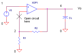
Let's jump right in and see what happens when hanging capacitance on an
op amp's output. op amp XOP1 has a gain of 2 and drives a
capacitive load CL. Run a simulation of OP_CLOAD.CIR and plot the input V(1)
and output V(4). Okay, things look pretty normal with
CL = 1 pF. But what happens if you start increasing CL to 10 pF, 100 pF, and
1000 pF or more? The desired output that previously changed quickly and
accurately, now unfortunately overshoots and rings for some time before
nearing its desired value.
OPEN-LOOP ANALYSIS
But why should a capacitive load push the circuit toward instability? To find out, let's apply one of our power tools - Open-Loop Feedback Analysis. This simple trick means opening up the feedback loop and checking for danger signs in the gain and phase around the loop. (For a review, see Opamp Feedback Analysis.)
Performing open-loop analysis requires these steps:
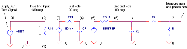
1. Short the voltage source, VS.
2. Open up the circuit.
3. Apply an AC test signal VTEST where the loop was opened and observe the AC gain and phase around the loop. If there is a frequency where the AC gain is 1 V/V (0dB) and the total phase is -360 or 0 deg, then the circuit is unstable (potential oscillations).
BREAK IT OPEN
Let's look at the entire loop including the op amp's innards modeled as single-pole amplifier. Note that breaking open the loop creates two nodes 20 and 2 where there was one. (The nodes in ( ) represent subcircuit nodes.)
What do you notice about ROUT and CL? Unfortunately, these components form a low-pass filter adding negative phase to overall loop, pushing the total toward -360 deg. Let's check out all the phase contributors.
| Components | Phase Contribution | Comment | |
| Op Amp Negative Input | -180 deg | A basic fact of negative feedback amplifiers. Inverting the signal results in an automatic -180 deg phase shift. | |
|
First Pole: RP1, CP1 |
-90 deg |
A low-pass filter (pole) in the op amp gain stage. |
|
| Second
Pole: ROUT and CL |
-90 deg | ROUT and CL form another low-pass filter (pole). |
As you can see, adding up the 3 phase contributors puts us right in
the heart of oscillation country,
-360 deg. Where do the two poles lie? The first-pole is created by the gain
stage.
fp1 = 1/( 2 ∙ π ∙ RP1 ∙ CP1)
= 1/( 2 ∙ π ∙ 1 kΩ ∙ 1.59 μF )
= 100 Hz
The second pole is created by the output components.
fp2 = 1/( 2 ∙ π ∙ ROUT ∙ CL)
= 1/( 2 ∙ π ∙ 100 Ω ∙ 1000 pF )
= 1.59 MHz
Remember, poles contribute -45 deg of phase at the cutoff frequency and -90 deg well above the cutoff frequency.
OPEN-LOOP TEST
Run an open-loop analysis using OP_LOAD_OL.CIR and plot the
AC magnitude VM(2) and
phase VP(2) around the loop. To get a better view, change the Y-axis
of VM(2) to a log scale and plot VP(2) in a separate window.
CIRCUIT INSIGHT With ROUT = 100 Ω and CL = 1 pF (essentially no capacitive load), find the frequency where the magnitude falls to 1 V/V (or 0 dB). Now, check the phase at this frequency. You should see the phase leveling out at -270 (or +90 deg) - a stable circuit! (You may have noticed that the SPICE waveform plotter sometimes automatically wraps around the phases from -180, -270, -360 over to +180, +90, 0 deg, respectively.)
Now, increase CL to 1000 pF or so. What happens at the 0 dB crossing? Curses! The phase starts falling toward -360 (or 0 deg) - potential instability! And the closer you get to -360 deg, the more your circuit will overshoot and ring! It appears that CL and ROUT have created an undesirable pole in your feedback loop. Wouldn't it be grand if we could cancel the effect of the ROUT, CL pole?
CAPACITIVE LOAD - A SOLUTION
How can we modify the circuit bring the phase under control? One way is by adding compensation components RC and CC.
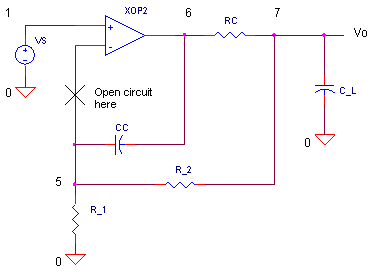
To see the benefit of RC and CC, let's look at he open loop circuit.
Capacitor CC helps by creating a high-pass filter counteracting the ROUT, CL low-pass filter! The net result is a positive phase contributor to cancel some negative phase. Also, RC helps by making CL look more resistive to ROUT at higher frequencies!
| Components | Phase Contribution | Comment | |
| Op Amp Negative Input | -180 deg | A basic fact of negative feedback amplifiers. Inverting the signal results in an automatic -180 deg phase shift. | |
|
First Pole: RP1, CP1 |
-90 deg |
A low-pass filter (pole) in the op amp gain stage. |
|
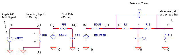
| Second
Pole: ROUT, CL |
-90 deg | ROUT and CL form another low-pass filter (pole). | |
|
Compensation Components: RC, CC |
+90 deg |
CC creates a zero in the loop. Finally, a positive phase contributor to compensate for the ROUT, CL low-pass filter. |
The good news is that the 4 phase contributors can put
us safety near
-270 deg. Let's run an open-loop analysis of our improved circuit
OP_LOAD_OL.CIR and plot the
AC magnitude VM(5) and phase
VP(5) around the loop. Set C_L to 1000 pF.
HANDS-ON DESIGN Let's see if RC and CC can bring the open loop plots under control. One rule of thumb says to start with RC = ROUT = 100 Ω and bump up CC until you find a phase response that stays near -270 deg ( +90 deg) at higher frequencies. Try values of CC between 100 - 1000 pF!
CLOSING THE LOOP
Although the open-loop AC response may look good, its better to close the loop and check its Transient Response to a step input.
HANDS-ON DESIGN With C_L = 1000 pF, RC = 100 and CC = 10 pF, run a simulation of OP_CLOAD.CIR and plot XOP2's output V(7). You may notice the output still rings and overshoots. Now keep bumping up the value of CC. You should see the output eventually brought under control! However, too much CC and the rise time slows too. You need to pick a value that strikes a compromise between a smooth response and a quick rise time.
Yes, RC and CC can save the day, but usually at the cost of less bandwidth. Another downside is that RC and CC are optimized for a particular load capacitance. Change the load capacitance, and the circuit response will also change.
SIMULATION NOTES
Get a refresher of Op Amp Feedback
Analysis techniques.
For a description of all op amp models, see
Op Amp Models.
For a quick review of subcircuits, check out
Why Use Subcircuits?
Get a crash course on SPICE simulation at
SPICE Basics.
A handy reference is available at SPICE
Command Summary.
Browse other circuits available from the Circuit
Collection page.
SPICE FILES
Download the file or copy this netlist into a text file with the *.cir extension.
OP_CLOAD.CIR - OPAMP WITH CAP LOAD - CLOSED-LOOP STEP RESPONSE
* STEP INPUT
VS	1	0	AC	1	PWL(0US 0V   0.01US 1V   10US 1V)
*
* CLOAD - NO COMPENSATION
R1	2	0	1K
R2	2	4	1K
XOP1	1 2	4	OPAMP1
CL	4	0	1PF

* CLOAD - COMPENSATION
R_1	5	0	1K
R_2	5	7	1K
XOP2	1 5	6	OPAMP1
RC	6	7	1
CC	6	5	1PF
C_L	7	0	1PF
*
*
* OPAMP MACRO MODEL, SINGLE-POLE
* connections:      non-inverting input
*                   |   inverting input
*                   |   |   output
*                   |   |   |
.SUBCKT OPAMP1      1   2   6
* INPUT IMPEDANCE
RIN	1	2	10MEG
* DC GAIN (100K) AND POLE 1 (100HZ)
EGAIN	3 0	1 2	100K
RP1	3	4	1K
CP1	4	0	1.5915UF
* OUTPUT BUFFER AND RESISTANCE
EBUFFER	5 0	4 0	1
ROUT	5	6	100
.ENDS
*
* ANALYSIS
.TRAN 	0.01US  2US
*
* VIEW RESULTS
.PLOT	TRAN 	V(4) V(7)
.PROBE
.END
Download the file or copy this netlist into a text file with the *.cir extension.
OP_CLOAD_OL.CIR - OPAMP WITH CAP LOAD - OPEN-LOOP FREQUENCY RESPONSE
*
VTEST	20	0	AC	1
*
* CLOAD - NO COMPENSATION
R1	2	0	1K
R2	2	4	1K
XOP1	0 20	4	OPAMP1
CL	4	0	1PF

* CLOAD - COMPENSATION
R_1	5	0	1K
R_2	5	7	1K
XOP2	0 20	6	OPAMP1
RC	6	7	1
CC	6	5	1PF
C_L	7	0	1PF
*
*
* OPAMP MACRO MODEL, SINGLE-POLE
* connections:      non-inverting input
*                   |   inverting input
*                   |   |   output
*                   |   |   |
.SUBCKT OPAMP1      1   2   6
* INPUT IMPEDANCE
RIN	1	2	10MEG
* DC GAIN (100K) AND POLE 1 (100HZ)
EGAIN	3 0	1 2	100K
RP1	3	4	1K
CP1	4	0	1.5915UF
* OUTPUT BUFFER AND RESISTANCE
EBUFFER	5 0	4 0	1
ROUT	5	6	100
.ENDS
*
* ANALYSIS
.AC 	DEC 	10 10 100MEG
*
* VIEW RESULTS
.PLOT AC	VM(2) VP(2)
.PROBE
.END
© 2004 eCircuit Center