Op Amp Limiter
CIRCUIT
OP_LIMITER1.CIR Download the SPICE file
Suppose you've been asked to limit the maximum output voltage of an amplifier. Why? Maybe the next stage will go up in smoke if its input swings beyond the maximum input rating. Or, maybe an op amp output gets frequently slammed into a rail by a big input signal. The recovery time can be long for some devices. To speed up recovery time, you can limit the output voltage level before saturation is reached. But how? A zener diode across the feedback resistor creates a fine limiting function. Unfortunately, for high precision applications, the non-ideal characteristics of the zener diode can wreck circuit accuracy. However, performance can be restored with a simple modification to the topology.
LIMITING ACTION
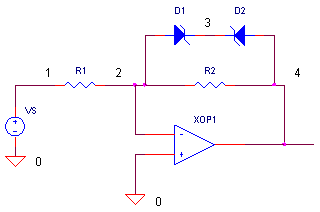
During normal operation (no limiting), the op amp works like your basic inverting amplifier. VS and R1 produce an input current I = VS / R1. (The negative input is at virtual ground, or 0V.) This same I flows through feedback element R2 to develop the output voltage, Vo = I ∙ R2. However, limiting occurs when the signal swings large enough to force D1 and D2 to conduct. For positive signals, the clip level begins at
V LIM POS = Vf D2 + VZ D1
where Vf D2 is the forward diode voltage of D2 and VZ D1 is the zener voltage of D1. Likewise, the negative clip level is set at
V LIM NEG = - ( Vf D1 + VZ D2 )
Above these levels the diodes conduct, clamping the output voltage to the same level.
CIRCUIT INSIGHT Run a simulation of OP_LIMITER1.CIR. Voltage source VS drives the input of inverting amplifier to 10 Vpeak for an expected output of -10 Vpeak. However, diodes D1 and D2 begin to conduct at V LIM POS or V LIM NEG, clipping the output at this level. To see the limiter in action, plot V(1) and V(4)
HANDS-ON DESIGN Pick another zener diode from the collection and place it in the circuit by typing a different model name in the diode statement. If both diodes D1 and D2 are the same device, you get symmetrical clipping. If you want asymmetrical clipping, pick two different devices for D1 and D2. Try putting in a single zener diode, what will output look like?
LEAKY DIODES
As expected, the world is an imperfect place, not the least being zener diodes. For reverse voltages below the zener voltage, you'd expect the zener diode to be OFF and essentially out of the circuit. Unfortunately, a small current leaks across the diode defined by the IS parameter in the diode model. For the 1N746, the reverse leakage is specified at ILEAK = 5 μA. This seemingly small leakage current can do nasty things to amplifier gain, especially at low voltages.
CIRCUIT INSIGHT Change the input level of VS to 0.5 Vpeak and replace D1 and D2 with the 1N746 devices. We could naively expect to see -0.5 V peak at the output, but we know better. Plot V(4) to see the less than spectacular gain performance due to zener leakage.
Only 0.45 V at the output! Why? Remember VS and R1 set up an input current I = 0.5V /
10 kΩ
= 50 uA.
Normally, this same I flows through R2 to develop the output Vo = 50
μA
∙ 10 kΩ = 0.5 V. However, not all of the
50 μA flows through R2. 5
μA leaks across the zener diode leaving only
45 μA through R2
to produce 0.45 V!
HANDS-ON DESIGN The larger the value of R1, the smaller the I, and the bigger an impact ILEAK has on the gain. Change R1 and R2 to something like 100 kΩ and watch the effect. Alternatively, choose smaller values of R1 and R2, 1 kΩ or so, to minimize the impact of zener leakage
ISOLATING LEAKAGE CURRENT
If reverse leakage is too troublesome, you can isolate it from the rest of the circuit. A simple addition of two ordinary diodes and a resistor can save the day.
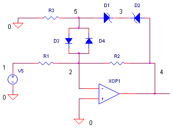
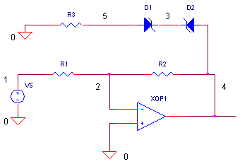
During normal operation (no limiting) the voltage across D3 and D4 is small. Why? First, the op amp's negative input is at virtual ground (0V). Second, voltage across R3 is merely the zener leakage current from flowing into R3, VR3 = 5 μA ∙ 10 kΩ = 50 mV. This small voltage leaves D3 and D4 OFF! And, because these diodes typically have small leakage currents, no significant current flows into the op amp's feedback element to disturb the gain. The circuit essentially looks like this.
Diodes D3 and D4 effectively isolate the zener diodes from the amplifier. However, when the output voltage swings beyond the following limits
V LIM POS = Vf D3 + Vf D2 + VZ D1
V LIM NEG = - ( Vf D4 +Vf D1 + VZ D2 )
the diodes begin to conduct, clamping the voltage across R2.
HANDS-ON DESIGN Enhance the design of the original circuit by adding D3, D4 and R3. The netlist should look something like
D1 5 3 D1N746
D2 4 3 D1N746
D3 5 2 D1N4148
D4 2 5 D1N4148
R3 5 0 10K
where the 1N4148 devices are ordinary diodes with relatively low leakage. Take the new circuit out for a spin with a 0.5 Vpeak voltage. Check out the gain. With R1 = R2 = 10 kΩ, does the output V(4) accurately follow V(1)? Increase R1 and R2 to 100 kΩ. Is your circuit still accurate? Now, turn up VS to 10V to see the diode chains swing into action.
SIMULATION NOTES
For a more detailed description of the op amp, see the Basic Op
Amp
Model.
For a quick review of subcircuits, check out Why Use Subcircuits?
SPICE FILE
Download the file or copy this netlist into a text file with the *.cir extension.
OP_LIMITER1.CIR - OPAMP WITH ZENER LIMITING
*
VS	1	0	SIN(0V 10VPEAK 1KHZ)
*
* INVERTING AMPLIFIER
R1	1	2	10K
R2	2	4	10K
XOP1	0 2	4	OPAMP1
*
* ZENER LIMITER
D1	2	3	D1N746
D2	4	3	D1N746
*
*
* ZENER DIODES
.model	D1N746	D(Is=5u Rs=14 Bv=2.81 Ibv=5u)
.model	D1N749	D(Is=1u Rs=11 Bv=3.82 Ibv=1u)
.model	D1N752	D(Is=0.5u Rs=6 Bv=5.20 Ibv=0.5u)
.model	D1N755	D(Is=0.05u Rs=3 Bv=7.11 Ibv=0.05u)
.model	D1N757	D(Is=0.05u Rs=5 Bv=8.67 Ibv=0.05u)
.model	D1N758	D(Is=0.05u Rs=9 Bv=9.49 Ibv=0.05u)
* DIODES
.model	D1N4148	D(Is=0.1p Rs=16 CJO=2p Tt=12n Bv=100 Ibv=0.1p)
*
*
* OPAMP MACRO MODEL, SINGLE-POLE
* connections:      non-inverting input
*                   |   inverting input
*                   |   |   output
*                   |   |   |
.SUBCKT OPAMP1      1   2   6
* INPUT IMPEDANCE
RIN	1	2	10MEG
* DCGAIN =100K AND POLE1=1/(2*PI*RP1*CP1)=100HZ
* GBP = DCGAIN X POLE1 = 10MHZ
EGAIN	3 0	1 2	100K
RP1	3	4	1000
CP1	4	0	1.5915UF
* OUTPUT BUFFER AND RESISTANCE
EBUFFER	5 0	4 0	1
ROUT	5	6	10
.ENDS
*
*
* ANALYSIS
.TRAN 	10US  1000US
*
.PROBE
.END
© 2003 eCircuit Center