Op Amp Input Offset Adjustment
CIRCUIT
OP_VOFF_ADJ.CIR Download the SPICE file
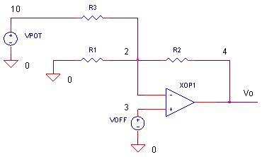
In some applications, the error due to Input Offset Voltage may be unacceptable. So how do you get rid of this error? One solution involves canceling it using another voltage of the same magnitude and opposite polarity. But the exact magnitude and polarity of the offset is unknown! You'll need a range of values (using a potentiometer, for example) to cover your basis.
ADDITIONAL ADJUSTMENT PATH
The question is how to get the canceling voltage into the circuit? One simple way is via a resistor R3 to the op amp's negative input. For simplicity, VPOT represents a voltage generated by a potentiometer divider circuit. The output due to VPOT is simply
Vo = VPOT ( -R2 /R3 )
which is the same equation as for the inverting amplifier.
HANDS-ON DESIGN Insert VPOT and R3 into the circuit by removing the * at the beginning of the statements. Run a simulation of OP_VOFF.CIR. Voltage VPOT generates a ramp that goes from -0.2V to +0.2 V. This simulates you turning the potentiometer over the full range. Check out the output voltage V(4). At some point, does the output get trimmed to 0 V?
Suppose you have a poorer grade op amp with a maximum offset of 5 mV. Change the VOFF value to 5MV. Run a new simulation. Does the output get trimmed to 0V? If not, increase VPOTs range beyond -0.2V to 0.2V. How big of a range to you need to cancel the 5mV offset. Another way you can adjust the cancellation range is to adjust R3. The equation above tells you that decreasing R3 increases the gain from VPOT to Vo.
HOW DOES R3 EFFECT GAIN?
What effect does R3 have on the gain of your circuit? That depends on which gain we're talking about. There are three gain of interest here. ( Notice that looking left from the op amps' negative input, R3 is effectively in parallel with R1.)
| Input Offset Voltage Gain | Vo / Voff = R2 / (R1||R3) + 1 | R3 directly effects the output error - the smaller the R3, the larger the error due to Voff. | |
| Non-Inverting Amplifier Gain | Vo / Vin = R2 / (R1||R3) + 1 | Feeding a signal to the op amp's positive input forms the non-inverting amplifier. The equation is identical to the one above. | |
| Inverting Amplifier Gain | Vo / Vin = - R2 / R1 | Feeding a signal to the left leg of R1 forms the inverting amplifier. R3 has no effect on this gain. |
CIRCUIT INSIGHT What are the above equations telling us? If you don't want your gain severely affected, keep R3 as large as possible. You can check the influence of R3 by setting VPOTs's ramp limits to 0V and 0V. Then, with R1 = 10k, R2 = 100k and VOFF = 1mV, the expected output error is 11 mV. Run a simulation to see how R3 = 1MEG or 100k changes the output voltage error?
OFFSET VOLTAGE DRIFT
Just because you trimmed out the offset voltage, doesn't mean all is tranquil on paradise island. The input offset voltage will drift with temperature; you have no control over this. But, knowing your overall error budget, you can select an op amp with a low enough offset drift for the intended temperature range.
INPUT BIAS CURRENT
Input offset voltage is not the only error of the op amp's input. The input stage is made of transistors, requiring a finite amount of bias current for operation. The circuit above assumes the bias is negligible. However, real op amps have bias currents to be reckoned with. The good news is there are clever techniques you can use to minimize and cancel out these errors too. (See Op Amp Input Bias Currents )
SPICE FILE
Download the file or copy this netlist into a text file with the *.cir extention.
OP_VOFF_ADJ.CIR - OPAMP OFFSET VOLTAGE
*
* AMPLIFIER CIRCUIT
*
R1	0	2	10K
R2	2	4	100K
XOP1	3 2	4	OPAMP1	;V+ V- VOUT
*
* OPAMP INPUT OFFSET VOLTAGE
VOFF	3	0	DC	1MV
*
* OFFSET COMPENSATION
* POTENTIOMETER DIVIDER - VPOT
VPOT	10	0	PWL(0MS -0.2V   10MS 0.2V)
R3	10	2	1MEG
*
*
* OPAMP MACRO MODEL, SINGLE-POLE
* connections:      non-inverting input
*                   |   inverting input
*                   |   |   output
*                   |   |   |
.SUBCKT OPAMP1      1   2   6
* INPUT IMPEDANCE
RIN	1	2	10MEG
* GAIN BW PRODUCT = 10MHZ
* DC GAIN (100K) AND POLE 1 (100HZ)
EGAIN	3 0	1 2	100K
RP1	3	4	1K
CP1	4	0	1.5915UF
* OUTPUT BUFFER AND RESISTANCE
EBUFFER	5 0	4 0	1
ROUT	5	6	10
.ENDS
*
* ANALYSIS
.TRAN 	0.1MS  10MS
* VIEW RESULTS
.PRINT	TRAN 	V(4)
.PROBE
.END
© 2002 eCircuit Center