Switched-Capacitor Integrator
CIRCUIT
SWCAP_INT.CIR Download the SPICE file
After discovering that a couple of switches and a capacitor can simulate a resistor (Switched-Capacitor Resistor), we can strap this circuit onto the front end of an op amp to create the basic building block of many filter circuits - the integrator. However, the major obstacle to happy filtering is the mine field of stray capacitance. These uncontrolled strays can add significant capacitance to the switched capacitor, destroying the accuracy of your desired filter response. But, help is on the way! By slightly modifying the way the capacitor is switched, the simulated resistor becomes immune to the surrounding strays.
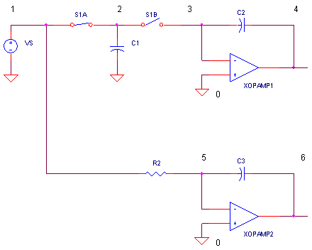
SWITCHED CAP INTEGRATOR
Let's replace the resistor of the Op Amp Integrator with a switched capacitor circuit. One end connects to the input voltage; the other feeds into the virtual ground of an op amp. (Virtual ground simply means that the op amp works to keep its negative input near ground, so the input ends up looking like a low impedance node at 0V.)
The operation is straight forward. Switches S1A and S1B are alternately closed and opened. With S1A closed, C1 charges up to Vin. Alternately, with S1B closed, C1 discharges into the virtual ground to 0V. But, where does this charge go? Because no current flows into the op amp, C2 receives the charge! How much?
Δq = ΔV ∙ C1 = Vin ∙ C1
Now if these switches are opened / closed at a regular time interval Δt, you get an average current flowing
i = Δq / Δt
= Vin ∙ C1 / Δt
Comparing this to ohms law we see a simulated input resistor of
R = Δt / C1
at the input of the op amp integrator.
INTEGRATOR TEST DRIVE
Switches S1A and S1B are turned ON and OFF every 10 μs by non-overlapping pulse generators VSA and VSB. Input voltage VS drives the integrator's input with a square wave that swings from +1 to -1 V every T = 100 μs. What kind of waveform can we expect at the output? A bipolar square wave at the integrator's input should generate a triangle wave at its output.
If you wanted a 1000 kΩ resistor at the integrator's input, what value of C1 do you choose?
C1 = Δt / R
= 10 μs / 1000 kΩ
= 10 pF
Before we test drive it, what should the triangle wave look like with Vin = 1V, R = 1000 kΩ, C2 = and 100 pF. After T = 100 μs the triangle wave should rise to
Vo = Vin / R ∙ T / C2
= 1 V / 1000 k ∙ 100 μs / 100 pF
= 1 V
CIRCUIT INSIGHT
Run a SPICE simulation of SWCAP_INT.CIR. First, let's see the
standard integrator circuit in action by plotting V(6). Okay, now let's look
at the switched-cap integrator at
V(4). Hey, check it out - the waveform is the same (almost)! The only
difference is that the switched-cap output rises in a stair-stepped
waveform. Why? The input current gets delivered in spikes as S1B is
repeatedly opened and closed. But on average, the same current flows into C2 as in
the standard integrator.
HANDS-ON DESIGN You can change the triangle wave by tweaking C1 up or down. Just remember to calculate the equivalent resistor for R2 if you want to compare the two integrators.
STRAY CAPS
Ready to throw some trouble into this circuit? Just add some stray capacitance across C1 by removing the "*" in front of CS1. It only takes a little stray capacitance to induce big errors when normal circuit values are in the 10 pF range. Rerun the simulation with C1 = 10 pF, CS1 = 2 pF and R1 = 1000 k. Did CS1 have a big impact on the output V(4)? Yes, 2 out of 10 pF can definitely rain on your filter parade.
So what's the solution to the stray cap problem? First, keep in mind that much of the stray capacitance appears from the switch nodes to ground. Second, what if we switched both ends of the circuit capacitor such that the strays never directly paralleled it. Here's one such circuit.
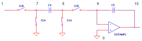
Although, a slightly different switch arrangement, this input delivers the same charge, Δq = Vin ∙ C, as the original circuit. When S2A and S3A close, there's 0V across the cap C4.
However, when S2B and S3B close, C4 charges to Vin. The accumulated charge on C4 must also flow into the virtual ground of the op amp and onto C5. But this circuit's main boasting rights come from being insensitive to the threats of stray capacitance. Of course, the cost to this benefit is a pair of additional switches.
CIRCUIT INSIGHT Run another simulation plotting both the standard integrator V(4) and improved integrator V(10). Okay, nothing new here. But now add stray capacitance to nodes 7 and 8 by removing the "*" in front of CS7 and CS8. The 2 pF at each end of C5 should have little impact on the output waveform! Increase CS7 and CS8 to 5 pF or more. Does any effect begin to show?
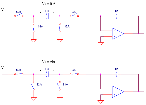
NON-INVERTING INTEGRATOR
Switched-capacitor circuits allow forms of trickery not possible with standard circuits. For example, you can transform this inverting integrator into a non-inverting one! Simply swap the intervals that S3A and S3B are turned ON and OFF. To do this, swap the nodes, 20 and 21, that control the switches by making their statements look like
S3A 8 0 21 0 SW1
S3B 8 9 20 0 SW1
Although the circuit works similarly as before, the charge on C4 is now directed to flow in the opposite direction into the op amp's virtual ground and onto C5.
HANDS-ON DESIGN Run a simulation with the new phases driving S3A and S3B. Plot the standard integrator V(4) and the modified integrator V(10). As advertised, the output of the non-inverting integrator should swing opposite of the standard integrator, its output now the same polarity as the input drive VS.
REFERENCES
Switched-Capacitor Circuit Design, R. Gregorian, et al, Proceedings of the IEEE, Vol 71, No. 8, August 1983.
SPICE FILE
Download the file or copy this netlist into a text file with the *.cir extension.
SWCAP_INT.CIR - SWITCHED-CAPACITOR INTEGRATOR
*
VS	1	0	PULSE(1V -1V 0US 0.1US 0.1US 100US 200US)
*
* SWCAP INTEGRATOR
S1A	1 2	20 0 	SW1
C1	2	0	10PF IC=0V
*CS2	2	0	2PF
S1B	2 3	21 0 	SW1
*
EOPAMP1	4 0	0 3	10000
C2	3	4	100PF
*
*
* OPAMP INTEGRATOR
R2	1	5	1000K
EOPAMP2	6 0	0 5	10000
C3	5	6	100PF IC=0V
*
*
* SWCAP INTEGRATOR - STRAY INSENSTIVE
S2B	1 7	21 0 	SW1
S2A	7 0	20 0 	SW1
*CS7	7	0	2PF
C4	7	8	10PF IC=0V
*CS8	8	0	2PF
S3A	8 0	20 0 	SW1
S3B	8 9	21 0 	SW1
*
EOPAMP3	10 0	0 9	10000
C5	9	10	100PF IC=0V
*
*
* SWITCH CONTROL - PHASE A AND B
V1A	20	0	PULSE(0V 5V 0US 0.01US 0.01US 2.5US 10US)
V1B	21	0	PULSE(0V 5V 5US 0.01US 0.01US 2.5US 10US)
*
.MODEL	SW1	VSWITCH(VOFF=0 VON=5 RON=10K ROFF=100MEG)
*
* ANALYSIS
.TRAN 	0.1US  400US
*
* VIEW RESULTS
.PRINT TRAN V(4) V(6) V(10)
.PROBE
.END
© 2004 eCircuit Center