Programmable Gain Amplifier (PGA)
CIRCUIT
OP_PGA.CR Download the SPICE file
The task at hand seems straightforward: read all of the system's sensors - thermistors, strain gauges, photodiodes - using a 12-bit ADC. But getting the most from an ADC means scaling the maximum signal from each sensor to match the maximum input of the ADC. How do you achieve this from sensors of vastly different signal strengths?
One indispensable circuit is the PGA - Programmable Gain Amplifier. The amplifier's gain can be conveniently changed via a small collection of analog switches, resistors and logic bits. Toggling these logic bits swaps resistors in the op amp's feedback network effectively changing the gain. As you might expect, there's several ways to accomplish this feat. In one configuration (PGA 1), the switch's ON resistance directly effects the gain. In a better version (PGA 2), the analog switches swap feedback resistors with minimal impact on gain.
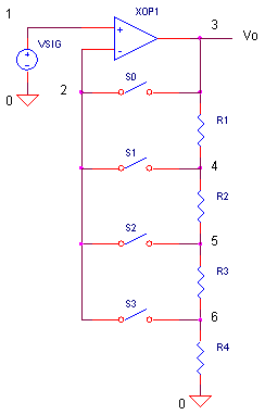
PGA - ROUND 1
Here's a typical PGA. Its operation is straight forward and intuitive.
This non-inverting amplifier changes its gain by closing switches S12, S13 and S14, one at a time, to change the feedback resistor network. The gain are easily calculated as
| Switch | Gain | |
| All OFF | 1 | |
| S12 = ON | R11 / (R12 +Ron) + 1 | |
| S13 = ON | R11 / (R13 + Ron) + 1 | |
| S14 = ON | R11 / (R14 +Ron) + 1 |
where Ron is the analog switch's ON resistance, typically 50 to 500 Ω. As you can see, Ron sits right in the middle of the gain equation. Why is this a problem? Unfortunately, Ron varies from device to device, it varies with temperature, and it varies with voltage level. If accuracy is required, Ron is not your ticket to ride.
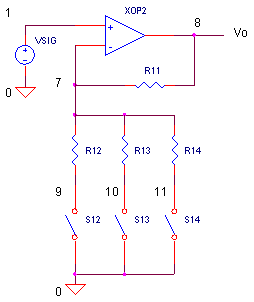
PGA - ROUND 2
Consider this approach to PGA design.
Like the previous non-inverting amplifier, it changes gain by individually closing switches. However, a closer look shows that no current flows through the analog switches. Why? Remember that one of the op amp's most desirable features is its negligible input current. This means there's no voltage across Ron! Therefore, if S1 closes, the voltage at node 4 appears at the op amp's negative input. The circuit essentially implements a non-inverting voltage gain of R1 / (R2+R3+R4). The gains for the each switch closure appears below.
| Switch | Gain | |
| S0 = ON | 1 | |
| S1 = ON | (R1) / (R2 + R3 + R4) + 1 | |
| S2 = ON | (R1 + R2) / (R3 + R4) + 1 | |
| S3 = ON | (R1 + R2 + R3) / (R4) + 1 |
You might notice what's missing from the equations - Ron!
PGA - POWER OF TWO
Typically, PGAs are designed in two varieties:
- powers of two (G = 1,2,4,...)
- powers of ten (G = 1,10,100,...)
Let's piece one together for gains of 1,2,4 and 8. What resistor collection provides these gains? One solution is R1 = 2 kΩ, R2 = 1 kΩ, R3 = 500 Ω and R4 = 500 Ω. This pattern can be extended to any number of gain ranges.
SPICE RUN (PGA 2)
SWITCH CONTROL - Four resistive switches S0-S3 are controlled by four voltages sources VS0-VS3 where the resistances Ron = 100 Ω and Roff = 100 MΩ are enabled by voltage levels Von = 5 V and Voff = 0V. The sources VS0 - VS3 each generate a 10 μs 5V pulse in four successive time slots. The bottom line? S0 closes during the first 10 us, S1 closes in the next 10 us, and so on. To produce an input test signal, VSIG generates its own 10 μs 1V pulse centered in each of 10 μs time slots.
CIRCUIT INSIGHT Run a SPICE simulation of OP_PGA.CIR. First, plot the control voltages for the four switches V(20), V(21), V(22) and V(23). Next, plot the input test pulses at V(1). Finally, check out the PGA 1 output by opening a new plot window and adding trace V(3). What do we expect here? The four input pulses at 1V appear amplified at the output as 1, 2, 4 and 8 V pulses according to the PGA's gain ranges.
Here's where this PGA stands tall among its peers. Increase or decrease the RON parameter by 2x in the SW1 model statement.
.MODEL SW1 VSWITCH(VON=5V VOFF=0V RON=100 ROFF=100MEG)
Rerun the simulation and check out V(3). The output levels remain rock solid even though Ron has changed significantly.
Question: what's happening to the rise time of each successive output pulse? The 8 V output pulse has a noticeably slower response than the 1 V output pulse. Why? The classic gain-bandwidth tradeoff comes into play here. If the gain goes up, the bandwidth (or speed) must come down.
SPICE RUN (PGA 1)
Let's give the first PGA 1 discussed above a chance to implement the same gains. Assuming Ron = 100 Ω and R11 = 2 kΩ, we can calculate R12 = 1.9 kΩ, R13 = 566.6 Ω and R14 = 185.7 Ω to give us gains of 1,2 4 and 8 V/V. Set RON = 100 and run a simulation, then plot this PGA's output V(8). Okay, so far so good - the output matches our champion PGA exactly.
However, what happens as we increase RON from 100 Ω to a value like 120 Ω? As you can see, this PGA's output V(8) loses its accuracy. Alternatively, the better design V(3) remains steadfast at the desired levels.
What's one possible solution to this RON problem? Choose R11 though R14 >> RON. Just be careful of how the op amp's input bias current may create a significant offset voltage in these resistors.
FURTHER ADVENTURES
HANDS-ON DESIGN In addition to gains of 1,2,4 and 8, suppose you needed a few more gains, like 16 and 32. How many additional switches are needed? What might resistor string look like?
What about a PGA whose gains are defined by powers of 10 such as 1, 10, 100 and 1000? What collection of resistors will get you there?
PARTING NOTES
Although our blue-ribbon PGA is insensitive to Ron, it is not without its own shortcomings. For one, it requires one more switch than the 2nd place finisher. Also, the gains are not independent of one another! Because each resistor plays a role in all of the gains, coming up with a resistor string for your desired gains can be tricky. The alternative PGA has all of its gains independent of one another. Setting arbitrary gains is a piece of cake.
Second, although we claimed that negligible current flows into an op amp, some finite current does flow. This input bias current, Ibias (not modeled here), flowing through Ron, creates an offset voltage that's amplified by the circuit's gain. You just need to pick Ron and Ibias such that the offset is small enough not to rain on your PGA parade. (See Input Bias Current)
In addition, Ron plus the switch's capacitance to ground at the op amp's input, create a low-pass filter in the feedback loop that may push the response towards ringing or oscillation. You may need a small capacitor across R1 to keep it stable. (See Feedback Analysis.)
You can also create an inverting PGA by starting with an inverting op amp configuration. But you might be stuck with Ron in the gain equation.
SIMULATION NOTES
For a more detailed description of the op amp, see the Basic Op
Amp
Model.
For a quick review of subcircuits, check out Why Use Subcircuits?
Get a crash course on SPICE simulation at
SPICE Basics.
A handy reference is available at SPICE
Command Summary.
Browse other circuits available from the Circuit
Collection page.
SPICE FILE
Download the file or copy this netlist into a text file with the *.cir extension.
OP_PGA.CIR - PROGRAMMABLE GAIN AMPLIFIER
*
* INPUT PULSES, ONE FOR EACH GAIN SETTING
VSIG	1	0	PULSE(0V 1V 2.5US 0.01US 0.01US 5US 10US)
*
* PGA 1
XOP1	1 2 3	OPAMP1
*
S0	3 2	20 0 	SW1
*
R1	3	4	2K
S1	4 2	21 0 	SW1
R2	4	5	1K
S2	5 2	22 0 	SW1
R3	5	6	500
S3	6 2	23 0 	SW1
R4	6	0	500
*
*
* PGA 2
XOP2	1 7 8	OPAMP1
*
R11	8	7	2K
*
R12	7	9	1.9K
S12	9 0	21 0 	SW1
R13	7	10	566.7
S13	10 0	22 0 	SW1
R14	7	11	185.7
S14	11	0	23 0 	SW1
*
*
* SWITCH CONTROL
VS0	20	0	PULSE(0V 5V 0US 0.1US 0.1US 10US 40US)
RS0	20	0	1MEG
VS1	21	0	PULSE(0V 5V 10US 0.1US 0.1US 10US 40US)
RS1	21	0	1MEG
VS2	22	0	PULSE(0V 5V 20US 0.1US 0.1US 10US 40US)
RS2	22	0	1MEG
VS3	23	0	PULSE(0V 5V 30US 0.1US 0.1US 10US 40US)
RS3	23	0	1MEG
*
.MODEL	SW1	VSWITCH(VON=5V VOFF=0V RON=100 ROFF=100MEG)
*
*
* OPAMP MACRO MODEL, SINGLE-POLE
* connections:      non-inverting input
*                   |   inverting input
*                   |   |   output
*                   |   |   |
.SUBCKT OPAMP1      1   2   6
* INPUT IMPEDANCE
RIN	1	2	10MEG
* DC GAIN=100K AND POLE1=100HZ
* UNITY GAIN = DCGAIN X POLE1 = 10MHZ
EGAIN	3 0	1 2	100K
RP1	3	4	100K
CP1	4	0	0.0159UF
* OUTPUT BUFFER AND RESISTANCE
EBUFFER	5 0	4 0	1
ROUT	5	6	10
*
.ENDS
*
* ANALYSIS
.TRAN 	0.5US 40US
*
* VIEW RESULTS
.PRINT TRAN	V(3) V(1)
.PROBE
.END
© 2005 - 2026 eCircuit Center