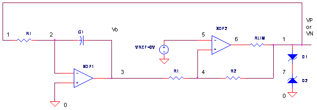
Op Amp Triangle-Wave Generator
CIRCUIT
OP_TRI_GEN.CIR Download the SPICE file
This signal generator gives you two waveforms for the price of one: a triangle-wave and a square-wave. What is the central component of this circuit? The integrator capacitor CI. Basically we are interested in performing two functions on CI: charge it, discharge it - repeat indefinitely. During the design process, we ask these essential questions
1. How do we charge/discharge CI?
2. How fast do we charge/discharge CI?
3. How do we switch from charging to discharging?
4. When do we switch from charging to discharging and visa-versa?
Most likely, there are scores of circuit options for every question. It all depends on the usual design context - budget, required accuracy, schedule, available components, personal experience and so on. Here's one simple incarnation of the triangle wave generator.
LINEAR RAMPS
How do we charge / discharge CI? A triangle wave implies that our circuit generates a linear voltage ramp. One way to achieve this goal is by charging / discharging CI with a constant current. The Op Amp Integrator provides a handy way to accomplish this. Here's a simplified version of the circuit.
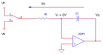
Ramp Up Connect RI to VN and what happens? With V- held at the virtual
ground (0V), a constant current flows from V- to VN.
Iin = VN / RI.
CI integrates Iin creating a positive linear ramp at Vo. The ramp is linear because Vo changes proportionally to the time elapsed ΔT.
ΔVo = - VN / (CI ∙ RI) ∙ ΔT
Ramp Down Connect RI to VP and a constant current flows from VP to V-,
Iin = - VP / RI. Now Vo ramps down linearly
ΔVo = - VP / (CI ∙ RI) ∙ ΔT
How Fast? To control the period of the generator, you need to answer this - how fast does Vo ramp up and down? Just look at the above equations and solve for ΔVo / ΔT.
Ramp Up:
ΔVo / ΔT
= - VN / ( CI ∙ RI
)
Ramp Down:
ΔVo / ΔT
= - VP / ( CI ∙ RI
)
These equations show you the parameters available to control the ramp up / down speeds.
UPPER AND LOWER BOUNDS
When do we switch from charging to discharging CI? Basically, you need to pick two levels - an upper and a lower threshold - to define the bounds of the triangle wave. The circuit ramps up or down, reversing at the upper and lower thresholds.
- With one leg of RI at VN, the output ramps up until the Upper Threshold ( Vth+ ) is reached. Then RI is switched from VN to VP.
- With one leg of RI at VP, the output ramps down until the Lower Threshold ( Vth- ) is reached. Then RI is switched from VP to VN.
COMPARATOR
And for our final question: how do we switch from ramping up to ramping down? Our goal is to replace the switch and VP/VN levels in the simplified circuit above. Here's one way to do it - an Op Amp Comparator with two thresholds. This simple yet wondrous circuit changes it's output state from VN to VP (or vise-versa) depending on the upper Vth+ and lower Vth- thresholds.
Vth+ = - VN ∙ R1 / R2
Vth- = - VP ∙ R1 / R2
How does it work?
- When Vin > Vth+, the output switches to VP, the POSITIVE output state.
- When Vin < Vth-, the output switches to VN, the NEGATIVE output state.
Zener diodes D1 and D2 set the positive and negative output levels:
VP = Vf D1 + VZ D2
VN = Vf D2 + VZ D1.
These output levels do double duty! Not only do they set the comparator thresholds, but also set the voltage levels for the next stage - the integrator.
TRIANGLE WAVE GENERATOR
HANDS-ON DESIGN Okay, time to design it, built it and simulate it! Suppose our design calls for a +/-10 V triangle wave, cruising along at 10 kHz. This means that Vth+ = +10 V and Vth- = -10 V. Given VP = +5 V, VN = -5 V, let's choose R2 = 10 kΩ and then calculate R1 = 20 kΩ from the equation above.
Now, if you have a 1 nF cap in stock, then what value of RI is needed for 10 kHz (T = 100 μs)? Because Vo needs to swing ΔVo = 10 - (-10) = 20 V in an interval ΔT = 50 μs, we solve the above equation in the Linear Ramps section for RI.
RI = (VP / CI ) ∙ (ΔT / ΔVo)
= (5 V / 1 nF) ∙ (50 μs / 20 V)
= 12.5 kΩ
Run a SPICE simulation of OP_TRI_GEN.CIR. Plot the triangle-wave output V(3) and the comparator output V(1). I don't know why, but I get a strange satisfaction out of watching the output ramping up and down on its own!
Want to speed up or slow down the action? Just change the current source level by doubling or halving RI. Run a new simulation and watch it go. Need a different peak to peak voltage swing? Simply raise or lower R1. But beware - changing the voltage thresholds also changes the time required to reach the thresholds. Also, make sure Vth+ and Vth- are not outside the +/-15V limits of the op amp model!
And don't forget the option of changing the reverse voltage of the zener diode via the BV parameter. Just remember the charging currents and thresholds will change too.
HOW ACCURATE?
You may have noticed that the triangle peaks and period may not accurately meet our +/-10V swing at 100 us. Why? The main reason is that our current source and thresholds are derived from zener diodes - not exactly the most accurate reference on the planet! You may need to spend a few bucks on trim pots for both R1 and RI. Other options for improving accuracy include bringing in some precision references for VP and VN. Some designs use improved means for deriving and switching the current sources that charge CI.
ASYMMETRICAL VOLTAGES
You can create asymmetrical voltage swings by including a reference voltage VREF to the comparator's negative input. (Actually, its been there all along, just set to 0V.) VREF let's you place the thresholds more freely - they can now both be positive or negative. Basically, VREF can shift the thresholds up or down as shown in the equation.
Vth+ = VREF ∙ (R1+R2)/R2 - VN ∙ R1 / R2
Vth- = VREF ∙ (R1+R2)/R2 - VP ∙ R1 / R2
HANDS-ON DESIGN Pick new thresholds by including VREF. For example, set R1 = R2 = 10k and VREF = 2.5 V. Run a new simulation and check your new triangle boundaries. Again, make sure your Vth+ and Vth- are not outside the +/-15V limits of the op amp model!
ASYMMETRICAL RAMPS
Good news! You're not confined to equal ramp up and down rates. For this trick, create a new voltage source VREF2 and connect it to the integrator's positive input. For example, add VREF and change XOP1 to look like this.
XOP1 9 2 3 OPAMP1
VREF2 9 0 2V
What does this do? Now you've got two different current-source levels to charge CI.
Iin+ = ( VP - V+) / RI.
Iin- = (VN - V+) / RI.
For example, set VREF2 to a voltage like 2V. With VREF2 = 2V, VP = 5V, VN = -5 V and RI = 12.5 kohms, you get unequal constant currents of Iin+ = -0.24 mA and Vin- = 0.56 mA. Rerun the simulation. You're triangle wave should start looking like sawtooth.
SIMULATION NOTES
The model for the op amp in this circuit includes a +/-15 V clamp accomplished by zener diodes. This models the limited voltage swing of a typical op amp. You can change this to reflect the supply rails and output limits of the op amp you are using.
To help our circuit start, we set the initial voltage of the CI to 0.1 V by the appending IC=0.1V to the CI statement. You could set it to some other voltage if you wish. Also, don't forget to tell SPICE to use this initial voltage by adding UIC (Use Initial Conditions) to the TRAN command.
Find out more about the Op Amp Comparator
and the Op Amp Integrator?
For a more detailed description of the op amp, see the Basic Op
Amp
Model.
For a quick review of subcircuits, check out Why Use Subcircuits?
SPICE FILE
Download the file or copy this netlist into a text file with the *.cir extension.
OP_TRI_GEN.CIR - OPAMP TRIANGLE GENERATOR
*
* INTEGRATOR
RI	1	2	12.5K
CI	3	2	0.001UF IC=0.1
XOP1	0 2 3	OPAMP1
*
*
* COMPARATOR WITH HYSTERESIS
R1	3	4	20K
R2	4	1	10K
XOP2	4 5 6	OPAMP1
RLIM	6	1	1000
D1	1	7	DZ1
D2	0	7	DZ1
*
* VREF
VREF	5	0	0V
*
*
* OPAMP MACRO MODEL, SINGLE-POLE WITH 15V OUTPUT CLAMP
* connections:      non-inverting input
*                   |   inverting input
*                   |   |   output
*                   |   |   |
.SUBCKT OPAMP1	    1   2   6
* INPUT IMPEDANCE
RIN	1	2	10MEG
* DC GAIN=100K AND POLE1=100HZ
* UNITY GAIN = DCGAIN X POLE1 = 10MHZ
EGAIN	3 0	1 2	100K
RP1	3	4	100K
CP1	4	0	0.0159UF
* ZENER LIMITER
D1	4	7	DZLIM
D2	0	7	DZLIM
* OUTPUT BUFFER AND RESISTANCE
EBUFFER	5 0	4 0	1
ROUT	5	6	10
*
* ZENER TO LIMIT OPAMP OUTPUT SWING (+/- 15v)
.model	DZLIM	D(Is=0.05u Rs=0.1 Bv=14.3 Ibv=0.05u)
.ENDS
*
* ZENER TO LIMIT COMPARATOR OUTPUT SWING
.model	DZ1	D(Is=0.05u Rs=0.1 Bv=4.3 Ibv=0.05u)
*
* ANALYSIS
.TRAN 	0.5US 300US UIC
*
* VIEW RESULTS
.PRINT TRAN	V(3) V(1)
.PROBE
.END
© 2005 eCircuit Center