Op Amp Differentiator
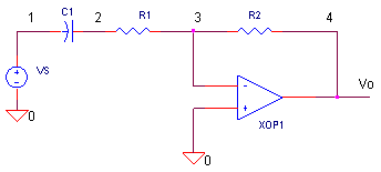
CIRCUIT
OPDFR.CIR Download the SPICE file
You probably recognize the differentiator - just one of many circuit possibilities - from your classic texts on op amps. Its number one function: create an output voltage proportional to the rate of change of the input voltage.
This leads to cool applications such as extracting edges from square waves, converting sinewaves into cosines and changing triangle waves into square waves.
But most circuits are susceptible to some trouble and this one is vulnerable to instability and noise. However, remedies are available to reduce the troubles without losing the desired function.
DIFFERENTIATOR
Ignoring R1 for a moment, let's look at the basic differentiator. How does this circuit respond to the rate of change of the input voltage?
Recall that the op amp's "prime directive" is to maintain 0 V (virtual ground) at its negative input. This places the input voltage VS across C1, producing an input current proportional to the rate of change of the input voltage.
i = C1 ∙ dVS / dt
Because no current flows into the op amp itself, i must flow through R2 creating the output voltage.
Vo = - i ∙ R2
Substituting for i we get
Vo = - C1 ∙ R2 ∙ dVS / dt
You may have noticed that the differentiator circuit looks a lot like its complementary companion, the integrator. The only difference being the swapped locations of the R and C (see Op Amp Integrator). These two circuits coexist like the Ying and Yang of the op amp universe.
TEST DRIVE
Run a TRAN simulation of OPDFR.CIR. Voltage source VS1 feeds a trapezoidal waveform to the differentiator's input. What can you expect at the output? With a 1 V rise in 10 ms, the output during this interval should be
Vo = - C1 ∙ R2 ∙ dVS1 / dt
= - 10 nF ∙ 500 kΩ ∙ 1 V / 10 ms
= - 0.5 V
HANDS-ON DESIGN Plot the transient response of V(1) and V(4). ( Remember it's an inverting configuration - positive slopes produce negative outputs.) What happens during the flat sections of the trapezoid? Need more output during the input's rising and falling edges? Just crank up C1 or R2. What happens when the speed of the edges changes? Increase or decrease the parameters Trise and Tfall in the waveform defined by the PULSE statement.
PULSE( V1 V2 Tdelay Trise Tfall Width Period )
The differentiator's output should change proportionally to the rise and fall times.
How about taking a sinewave (VS2) to the differentiator's input. Comment out VS1 by placing a "*" at the beginning of its statement. And insert VS2 by removing its "*". What waveform do we expect at the differentiator's output? If VS = A ∙ sin (ω ∙ t), then dVS / dt = ω ∙ A ∙ cos ( ω∙ t ). Extending this equation to the circuit, we get
Vo = - C1 ∙ R2 ∙ dVS / dt
= - C1 ∙ R2 ∙ ω ∙ A ∙ cos ( ω ∙ t )
= -10 nF∙500k∙(2∙3.14∙20 Hz)∙1V∙cos (ω∙t)
= - 0.628V ∙ cos ( ω ∙ t )
Rerun the simulation. Does V(4) match the equation's prediction? When interpreting these waveforms, I sometimes get confused because of the minus sign. It helps if I plot -V(4) instead. This way I can think in terms of the pure derivative without the inversion.
WHY RESISTOR R1?
CIRCUIT INSIGHT Op amp circuits, like any feedback circuit, are susceptible to the hazards of connecting the output back to its own input - ringing and oscillation. Enter R1 to rescue this circuit. How bad can things get? With C1 = 10 nF, R2 = 500 k and R1 = 5 k, try removing R1 (set it to 0.1 ohm) watch the show at V(4).
How does R1 remedy the ringing? In a nutshell, the main cause of instability is C1 in the feedback path, especially at high frequencies. So let's include R1. Now, at high frequencies C1 looks like a short compared to R1. Essentially, all that remains in the feedback path are resistors R1 and R2. The circuit now looks like your basic stable inverting amplifier.
But how does C1 cause the output spin out of control? By using a simple tool - Open-Loop Analysis - we can spot the causes ringing and oscillation. In an upcoming topic, we perform open-loop analysis on the differentiator, why it rings and how to fix it.
FREQUENCY RESPONSE AND NOISE
Looking at the differentiator's frequency response, you'll find that its output increases linearly as frequency increases. Comment out VS1 and VS2 by placing a "*" at the beginning of their statements. And insert AC source VS3 by removing its "*".
CIRCUIT INSIGHT With C1 = 10 nF, R2 = 500 k and R1 = 5 k, run a simulation and plot the AC response at V(4). Change the Y axis to a log scale, to get a better view. The output should rise as frequency increases. Unfortunately, noise usually crackles and snaps at higher frequencies producing outputs from the differentiator where the noise can obscure the signal!
There's another interesting feature - what happens at high frequencies? It looks like the gain maxed out at 100 V/V. Why? With C1 looking like a short at high frequencies, the resulting inverting configuration amplifies the signal by a maximum of -R2 / R1 = -500 k / 5 k = -100 V/V. However, this maximum actually benefits us, limiting the gain available to higher frequency noise! The downside is the limit on the maximum rate of change to which the differentiator can respond.
Looking at even higher frequencies, the output begins to fall. This is where the op amp device itself runs out of gas because of its own limited bandwidth.
SIMULATION NOTES
Check out the differentiator's companion circuit, the
Op Amp Integrator.
For a description of all op amp models, see
Op Amp Models.
For a quick review of subcircuits, check out
Why Use Subcircuits?
Get a crash course on SPICE simulation at
SPICE Basics.
A handy reference is available at SPICE
Command Summary.
Browse through other circuits available from the Circuit
Collection page.
SPICE FILE
Download the file or copy this netlist into a text file with the *.cir extension.
OPDFR.CIR - OPAMP DIFFERENTIATOR
*
* TRAPEZOIDAL WAVE
VS1	1	0	PULSE(0V 1V 0MS 10MS 10MS 10MS 40MS)
* SINEWAVE
*VS2	1	0	SIN(0VOFF 1VPEAK 20HZ)
* 1 VRMS FOR AC ANALYSIS
*VS3	1	0	AC	1
*
C1	1	2	10NF
R1	2	3	5K
R2	3	4	500K
XOP	0 3	4	OPAMP1
*
*
* OPAMP MACRO MODEL, SINGLE-POLE
* connections:      non-inverting input
*                   |   inverting input
*                   |   |   output
*                   |   |   |
.SUBCKT OPAMP1      1   2   6
* INPUT IMPEDANCE
RIN	1	2	10MEG
* DCGAIN =100K AND POLE1=1/(2*PI*RP1*CP1)=100HZ
* GBP = DCGAIN X POLE1 = 10MHZ
EGAIN	3 0	1 2	100K
RP1	3	4	1000
CP1	4	0	1.5915UF
* OUTPUT BUFFER AND RESISTANCE
EBUFFER	5 0	4 0	1
ROUT	5	6	10
.ENDS
*
* ANALYSIS
.TRAN 	1MS  100MS
*
* VIEW RESULTS
.PROBE
.END
© 2004 eCircuit Center