2nd Gain Stage
CIRCUIT
OPMODEL3_2ND_GAIN_STAGE.CR Download the SPICE file
Unfortunately, for particular combinations of slew-rate, first-pole frequency and open-loop gains, the Intermediate Op Amp Model just can't handle it. The spreadsheet coughs up a negative number for RE1 and RE2 making it impractical. So what's the fix? Normally all of the gain comes from the same stage that models the first pole frequency and slew rate. But, what if we split the gain into the two stages, by adding another gain stage? This additional stage also comes with a key ingredient - a voltage clamp to set the slew-rate. This additional degree of freedom makes any combination of slew-rate, pole frequency and gain possible. A spreadsheet below helps you arrive at the component values. If you wish, take a quick refresher tour of the Intermediate op amp Model.
KEY FEATURES
For this op amp model, there are several key characteristics.
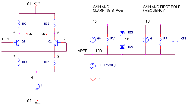
» The voltage gain of differential amplifier and output buffer is unity.
» The voltage gain is provided by by two stages:
1) the Gain / Voltage Clamping Stage - GV, RV
2) the Gain / First-Pole Stage - G1, RP1.» The slew-rate limiting is accomplished by a voltage clamp in the additional gain stage
that subsequently limits the peak current delivered to capacitor CP1.
OVERALL VOLTAGE GAIN
From differential input to output buffer, you can write the gain as
Aol = KDIFF ∙ KV ∙ KG ∙ KBUFF
where
| Term | Stage | Voltage Gain | Comment | |
| KDIFF | Differential amp | RC1 / (RE1 + 1/gm) | Typically set to 1 | |
| KV | Voltage gain of the additional stage. | KGV ∙ RV | Set gain in the 100s or so. | |
| KG | Standard voltage gain stage. | KG1 ∙ RP1 | The gains of
both stages KV ∙ KG sets the open-loop gain. |
|
| KBUFF | Output buffer | KEBUF | Typically set to 1 |
KGV is the gain in A / V of GV, a Voltage-Controlled Current Source (VCCS).
KG1 is the gain in A / V of G1, a Voltage-Controlled Current Source (VCCS).
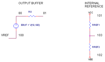
KEBUF is the gain in V / V of EBUF, a Voltage-Controlled Voltage Source (VCVS).
THE TEST
The Intermediate Model works only if it passes the following test:
![]()
For combinations of high slew-rate and first pole frequency, the test returns a NO. As a result, RE1 and RE2 become negative and we put the model out with the trash. However, an additional gain stage and voltage clamp transforms this model into a useful one.
GAIN AND SLEW-RATE LIMITING
How did slew-rate limiting work in the Intermediate Model? Essentially, the clamping (or limiting) action was accomplished by the differential pair. Normally the pair's bias current I1 is split between the two transistors. However, when the input is overdriven, all of I1 flows into one transistor only. This maximum current I1 is delivered to capacitor CP1 via G1 limiting the rate at which it could charge.
However, our new model places the limiting action in the additional gain stage. Zener diodes DZ1 and DZ2 clamp the voltage to a maximum of VCLAMP = VD_ZENER + VD_ON. This maximum voltage produces a peak current in G1 and slew-rate limit of

The only trick is choosing a gain KV for this additional stage. With too little gain, the limiting action of the differential amplifier will clamp V(15) before the VCLAMP voltage. So you need enough gain KV for the clamp diodes kick in first. A few iterations with the spreadsheet may be needed to get the gain high enough.
The overall gain of the op amp model (open-loop gain) is given by
AOL_DC = KV ∙ KG
= (KGV∙ RV)∙( KG1∙ RP1)
OP AMP COMPONENT VALUES
A few simple calculations and your model is ready.
1. Pick a gain for the intermediate stage, in the range of 200 - 500 or so.
KV = 200
Choose RV and KGV to make KV = 200. Typical example: If KGV = 0.001, then
RV = KV / KGV = 200 kΩ.
2. Select a value for RP1. A value around 1M is a typical value.
RP1 = 1M
3. Calculate KG1 to provide for the open-loop voltage gain.
4. Find the first-pole frequency fp1 from the op amp's gain AOL_DC and the
Unity-Gain Frequency fu (also equal to the Gain-Bandwidth Product GBP.)
5. Calculate CP1 to achieve fp1
6. Calculate VCLAMP which limits the peak current into CP1 via G1 causing the desired slew-rate limit.
Set the zener voltage of the clamp diodes
VD_ZENER = VCLAMP - 0.6 V
via the BV parameter (Breakdown Voltage) in the diode model statement.
7. Choose the bias current I1 for the differential amp for a convenient value - possibly something less than the op amp's total quiescent current.
I1 = 1 mA, 100 uA or 10 uA, etc.
8. Choose a value for RE1 and RE2, around 10 - 100 or so. (You may need to adjust RE1, RE2 and I1such that maximum voltage at the intermediate stage V(15), without the diode clamps, is greater than the VCLAMP.)
RE1 = RE2 = 100
9. Calculate RC1 and RC2 for unity gain at the differential amp
RC1 = RE1 + 1/gm
where
gm = IE1 / VT = ( I1 / 2 ) / VT and VT = 25.85 mV at 27 ° C
10. Time for a reality check! Is the maximum voltage at V(15), due to the limiting action of differential input, greater than VCLAMP. If not, V(15) will never reach VCLAMP. The maximum output of the differential amp is V(5,6)max = I1 ∙ RC1. So the maximum voltage at V(15) becomes
- If V(15)max > VCLAMP, all is well and the model is flight ready.
- If V(15)max < VCLAMP, you need to play with RE1, I1 and/or KV to
get V(15)max above VCLAMP.
11. Lastly, this model has an input bias current because of its transistor input stage. By setting the transistor's current gain β, you establish the input bias current Ibias.
β = Ibias / ( I1 / 2 )
The current gain β appears in the transistor model as parameter BF.
.model NPN NPN(BF=50000)
► EXCEL SPREADSHEET AND EXAMPLE
To help calculate the component values, you can download an Excel spreadsheet Opamp Parameters - 2nd Gain Stage.xls. The example is for an op amp with the following specs:
- AOL_DC = 100k V/V ( Open-Loop DC Gain )
- fu = 200 MHz ( Unity Gain Frequency or Gain Bandwidth Product )
- fp1 = 2 kHz ( First-Pole Frequency )
- SlewRate = 40 V/μs ( Slew Rate Limit )

OP AMP TEST DRIVE
OPEN-LOOP RESPONSE Let's take a look at the open-loop response of the SPICE file OP3_2ND_GAIN_STAGE.CIR. VS drives the positive input; R1 = 1 Ω grounds the negative input.
Run an AC Analysis and plot the output V(3). How does the op amp model perform? Is the low frequency gain equal to AOL_DC = 100k V/V? To get a better view, change the Y-Axis Settings to a log scale. Does the output fall to 0.707 of maximum at fp1 = 2000 Hz? And finally, does the output drop to unity at fu = 200 MHz?
CLOSED-LOOP RESPONSE Time to strap some feedback around our op amp model and check its response to a step input.
For a non-inverting amplifier with unity gain, remove R1 by adding a "*" at the beginning of its statement and add R2 = 1 Ω by removing the "*" at the beginning of its statement. VS generates a 1 V step input voltage. Run an Transient Analysis and plot the input V(1) and output V(3).
CIRCUIT INSIGHT How does the model's slew-rate limit measure up to the expected 40 V/μs? To check it, see if the output ramps to 0.4 V in 10 ns, which represents the same slew-rate limit. During the slewing action, take a look at the clamping action at V(15) of the model. Although inside the subcircuit, your display program should let you plot voltages within a subcircuit.
HANDS-ON DESIGN Suppose your asked to create a model of the following op amp:
- AOL_DC = 500 kV/V ( Open-Loop DC Gain )
- fu = 100 MHz ( Unity Gain Frequency or Gain Bandwidth Product )
- fp1 = 200 Hz ( First-Pole Frequency )
- SlewRate = 25 V/μs ( Slew Rate Limit )
Run the parameters of this op amp (or any other op amp you choose) through the Excel spreadsheet. You should be able to create a SPICE model for the basic behaviors of most op amps.
SIMULATION NOTES
Take a quick refresher tour of the
Intermediate Op Amp Model.
For a description of all op amp models, see
Op Amp Models.
For a quick review of subcircuits, check out
Why Use Subcircuits?
Get a crash course on SPICE simulation at
SPICE Basics.
A handy reference is available at SPICE
Command Summary.
To see how open-loop gain and bandwidth influence closed-loop bandwidth, see
Op Amp Bandwidth.
This model can be used with many of the op amp circuits available from the
Circuit Collection page.
SPICE FILE
Download the file or copy this netlist into a text file with the *.cir extension.
OPMODEL3_2ND_GAIN_STAGE - OPAMP MODEL WITH 2ND GAIN STAGE.CIR
*
* SIGNAL SOURCE
VS	1	0	AC 1	PWL(0US 0V   0.01US 1V  100US 1V)
*
* POWER SUPPLIES
VCC	10	0	DC	+15V
VEE	11	0	DC	-15V
*
*R1	0	2	1
R2	2	3	1
XOP	1 2 3  10 11	OPAMP3
RL	3	0	100K
*
* OPAMP MACRO-MODEL 3 - ADDITIONAL GAIN STAGE
*
*                IN+ IN- OUT  VCC  VEE
.SUBCKT OPAMP3   1   2   81   101   102
Q1	5 1	7	NPN
Q2	6 2	8	NPN
RC1	101	5	151.7
RC2	101	6	151.7
RE1	7	4	100
RE2	8	4	100
I1	4	102	0.001
*
* ADDED GAIN STAGE
GV	100 15	6 5	0.001
RV	15	100	200K
* CLAMP FOR SLEW-RATE LIMITING
DZ1	15	16	DZENER
DZ2	100	16      DZENER
*
* GAIN, FIRST-POLE AND SLEW RATE
G1	100 10	15 100 0.0005
RP1	10	100	1MEG
CP1	10	100	79.6PF
*
*OUTPUT STAGE
EOUT	80 100	10 100	1
RO	80	81	100
*
* INTERNAL REFERENCE
RREF1	101	103	100K
RREF2	103	102	100K
EREF	100 0	103 0 1
R100	100	0	1MEG
*
.MODEL NPN  NPN(BF=50000)
.MODEL DZENER D(BV=5.7V IS=1E-14 IBV=1E-3)
*
.ENDS
*
* ANALYSIS
.TRAN 	0.001US  0.2US
.AC 	DEC 	5 1HZ 1000MEGHZ
*
* VIEW RESULTS
.PRINT	TRAN 	V(3)
.PRINT	AC 	V(3)
.PROBE
.END
REFERENCES
SPICE-Compatible Op Amp Macro-Models, M. Alexander, D. Bowers, Analog Devices, Application Note AN-138, 1990.
OP-470 SPICE Macro-Model, J. Buxton, Analog Devices, Application Note AN-132, 1990.
© 2003 eCircuit Center