Output Current Limiting
CIRCUIT
I_LIMIT.CIR Download the SPICE file
In haste to complete a circuit, I've often overlooked specifications on a data sheet including an op amp's maximum output current. But the op amp dutifully performs as designed. Hopefully sooner than later, I'll discover the shortcoming in the output drive and remedy the situation with a change of circuit or device.
First we'll develop a basic current limit model for SPICE, and then we'll strap it onto the Intermediate Op Amp Model. We'll see how quickly the available current can be consumed by not only the load impedance, but the op amp's own feedback components as well!
OUTPUT CURRENT LIMIT
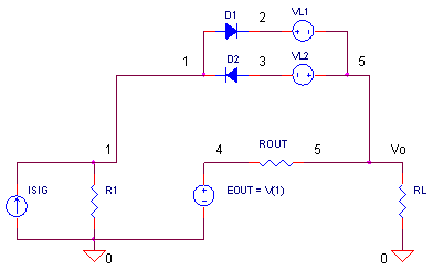
How do we get SPICE to mimic the output current limit action? In the circuit above, let's temporarily ignore components D1, D2 and VL1,VL2. What remains is a couple of basic op amp stages. Current source ISIG and R1 represent your typical gain stage while EOUT and ROUT represent a typical output stage. Under normal operation EOUT simply buffers the voltage across R1.
But what happens when the current limiting components get added? As more current is demanded by RL, the voltage across ROUT increases. However, a point is reached where the D1, VL1 pair begin to conduct, clamping the voltage between V(1) and V(5) to a maximum set according to
Vcl = VD1 + VL1
But remember EOUT forces V(4) = V(1), so the clamping action also constrains V(4) and V(5) to this same Vcl! The end result is a maximum output current that can flow through ROUT equal to
I_ROUT_max = Vcl / ROUT
= ( VD1_max + VL1) / ROUT
For opposite polarity swings, the operation is the same utilizing D2 and VL2.
COMPONENT CALCULATIONS
So what's the maximum current out of the device. Let's look at the output stage during current limiting.
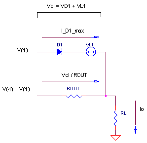
Notice, there's actually two components in the output current - one through ROUT and the other sneaks though clamp VD, VL1. What is this current through D1 and VL1? Remember ISIG flows through D1 during limiting action. Therefore, the total output current becomes
Io_max = I_ROUT_max + I_D1_max
= ( VD1_max + VL1 ) / ROUT + I_ISIG_max
(Actually, not all of ISIG flows through D1 and VL1. An insignificant current, V(1) / R1, flows through R1 as long as V(1) is relatively small and R1 is relatively large.)
So how do we choose our components? Simply determine the VD1_max and then calculate VL1. For the diode, we write

where
Id - diode current
Vd - diode voltage
IS - diode saturation current
Vt - thermal voltage (constant)
Solving for Vd, we get
![]()
In the above equation, replacing Id = I_D1_max gets you Vd = VD1_max. Now, you can solve for VL1 in the limiting equation.
VL1 = ( Io_max - I_D1_max )∙ROUT - VD1_max
► EXCEL SPREADSHEET AND EXAMPLE
To help calculate component values, you can download an Excel spreadsheet I_Limit.xls. The example calculates the components for the following current limit:
- Io_max = 10 mA ( Max Output Current )
- I_D1_max = 1 mA ( Max diode Current )
- I_ROUT_max = 9 mA ( Max ROUT Current limited by D1 and VL1)
- ROUT = 100 Ω
- Vcl = 0.9 V (Clamp voltage required for current limit.)
- IS = 1E-15 ( Diode Saturation Current )
Running through the spreadsheet, we get VD1_max = 0.714 V and VL1 = 0.186 V for a total clamp voltage of Vcl = 0.9 V. This allows a maximum output current of
Io_max = ( 0.714 V + 0.186 V ) / 100 Ω + 1 mA
= 9 mA + 1 mA
= 10 mA
CURRENT LIMIT CIRCUIT
In the circuit at the top of the page, ISIG generates a 1 mA peak sinewave into R1 = 100 kΩ producing a 100V peak voltage at V(1). EOUT buffers the voltage at V(1) through ROUT = 100 Ω.
CIRCUIT INSIGHT Simulate the SPICE file I_LIMIT.CIR and plot the output V(5). With the output limited to 10 mA and loaded by RL = 1000 Ω, how high a voltage do you expect at V(5)? What is Vcl at V(5,1)?
Open a new plot window and plot the output current I(RL). Does the limiter do an accurate job? Check the output stage's currents by adding traces I(D1) and I(ROUT). Do they add up to I(RL)? Decrease RL. Does the output maintain its current limit?
HANDS-ON DESIGN Choose different circuit parameters like ROUT = 75 Ω and Io_max =20 mA. Design a new limiting circuit using the Excel spreadsheet and rerun the simulation. How close to 20 mA does the output get limited?
OP AMP MODEL WITH CURRENT LIMIT
Okay, let's add current limiting circuit to our Intermediate op amp Model.
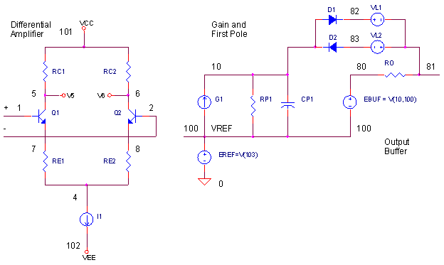
Similar to the initial example, the output is designed for RO = 100 Ω and Io_max = 10 mA. What's the maximum current out of G1? For this op amp model, with its input overdriven, all of the differential amp's bias current (I1 = 1 mA ) will flow through G1 and subsequently through D1, VL1 during the positive current limit condition. (For other op amp models, you need to determine the max current available from the last gain stage or frequency shaping stage.)
CURRENT LIMIT TEST DRIVE
Let's test our new op amp model in a typical application - the non-inverting amplifier.
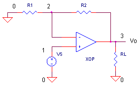
VS generates a 10 Vpeak input triangle wave to the amplifier strapped for
a gain of
+ 2 V/V (R1 = R2 = 100 kΩ).
CIRCUIT INSIGHT
Run the SPICE file OPMODEL3_I_LIMIT.CIR. For RL = 10 kΩ, the output
at V(3) should swing the full 20 V peak.
But what happens to V(3) when the load is lowered to
RL = 1 kΩ? Open a new plot window and check the current
limit by adding trace I(RL).
Now, try lowering the feedback resistors to
R1 = R2 = 1 kΩ. Rerun the simulation and
check
out I(RL). Why is it less - did the current limit change? The answer is no,
the max output current remains the same (10 mA). However, some of the
current is consumed by the feedback resistors R1 and R2. We just didn't
notice it before when R1 and R2 were both large! Add I(R2) to account
for the missing current. Lesson learned: the
op amp's output current must supply not only the load, but its own feedback
resistors as well!
SIMULATION NOTES
Take a quick refresher tour of the
Intermediate Op Amp Model.
For a description of all op amp models, see Op
Amp Models.
For a quick review of subcircuits, check out
Why Use Subcircuits?
Get a crash course on SPICE simulation at
SPICE Basics.
A handy reference is available at SPICE
Command Summary.
To see how open-loop gain and bandwidth influence closed-loop bandwidth, see
Op Amp Bandwidth.
This model can be used with many of the op amp circuits available from the
Circuit Collection page.
SPICE FILES
Download the file or copy this netlist into a text file with the *.cir extension.
I_LIMIT.CIR - CURRENT LIMIT
*
* SINEWAVE - 1 MA PEAK x 100K = 100 V PEAK
ISIG	0	1	SIN(0 1MA 1KHZ)
R1	1	0	100K
*
* OUTPUT STAGE
EOUT	4 0	1 0	1
ROUT	4	5	100
RL		5	0	1000
*
* CURRENT LIMIT
D1	1	2	DILIM
VL1	2	5	DC	0.186V
D2	3	1	DILIM
VL2	5	3	DC	0.186V
*
.model	DILIM	D(IS=1E-15)
*
* ANALYSIS
.TRAN 	0.01MS  1MS
*
* VIEW RESULTS
.PRINT	TRAN 	V(5)
.PROBE
.END
Download the file or copy this netlist into a text file with the *.cir extension.
OPAMP3_I_LIMIT.CIR - OPAMP MODEL WITH OUTPUT CURRENT LIMITING
*
* SIGNAL SOURCE - TRIANGLE WAVE
VS	1	0	PWL(0MS 0V   25MS 10V  75MS -10V   100MS 0V)
*
* POWER SUPPLIES
VCC	10	0	DC	+15V
VEE	11	0	DC	-15V
*
R1	0	2	100K
R2	3	2	100K
XOP	1 2 3  10 11	OPAMP3
RL	3	0	10000
*
*
* OPAMP MACRO MODEL (INTERMEDIATE LEVEL)
* WITH OUTPUT VOLTAGE LIMITING
*                IN+ IN- OUT  VCC  VEE
.SUBCKT OPAMP3   1   2   81   101   102
Q1	5 1	7	NPN
Q2	6 2	8	NPN
RC1	101	5	95.49
RC2	101	6	95.49
RE1	7	4	43.79
RE2	8	4	43.79
I1	4	102	0.001
*
* OPEN-LOOP GAIN, FIRST POLE AND SLEW RATE
G1	100 10	6 5 0.0104719
RP1	10	100	9.549MEG
CP1	10	100	0.0016667UF
*
* CURRENT LIMIT
D1	10	82	DILIM
VL1	82	81	DC	0.186V
D2	83	10	DILIM
VL2	81	83	DC	0.186V
.model	DILIM	D(IS=1E-15)
*
*OUTPUT STAGE
EOUT	80 100	10 100	1
RO	80	81	100
*
* INTERNAL REFERENCE
RREF1	101	103	100K
RREF2	103	102	100K
EREF	100 0	103 0 1
R100	100	0	1MEG
*
.model NPN  NPN(BF=50000)
*
.ENDS
*
* ANALYSIS
.TRAN 	1MS  100MS
*
* VIEW RESULTS
.PRINT	TRAN 	V(3)
.PROBE
.END
REFERENCES
SPICE-Compatible Op Amp Macro-Models, M. Alexander, D. Bowers, Analog Devices, Application Note AN-138, 1990.
© 2004 eCircuit Center