Supply Rail Correction Current
CIRCUIT
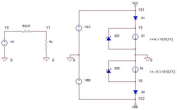
I_SUPPLY.CIR Download the SPICE file
One shortcoming of our behavioral op amp model developed so far, is the accuracy of the current drawn from the power supply pins - especially as a consequence of the load current. In our model, the output stage is referenced ultimately to ground. The result? The load current never flows though the supply rails! (In other op amp incarnations, the output current flows equally through both the positive and negative rails - also inappropriate!) But we know the current flows through only one or the other supply pin, depending if its sourcing or sinking current. The challenge is to develop an auxiliary circuit to make a correction current at the supply pins to reflect the current draw of a real output stage.
OUTPUT CURRENT AND SUPPLY PINS
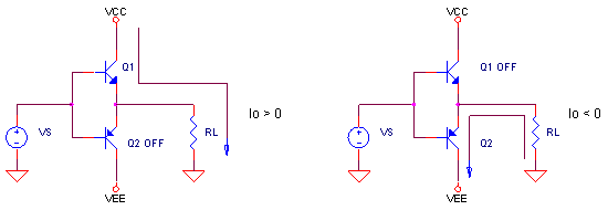
In a real op amp, the output stage is made up of transistors, typically in a push-pull arrangement. Current naturally flows through the positive supply pin only for positive outputs and vice-versa for negative output currents.
CORRECTION CURRENT
Unfortunately, the current from the output stage of our op amp model does not flow through either rail. To correct this, we'll hang a SPICE circuit across the rails that push an equivalent current through the appropriate rail. Current source G1 mirrors the output current Io through ROUT. Similarly, G2 mirrors the output current, but in the opposite polarity. Then, it's up to the diode networks to steer the current to the proper rail given the polarity of the output current.
 |
 |
|
|
POSITIVE OUTPUT CURRENT (SOURCING) |
NEGATIVE
OUTPUT CURRENT (SINKING) |
|
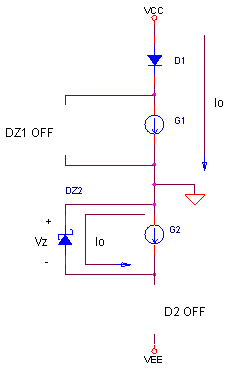
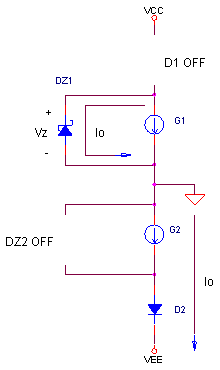
| G1 and D1 force a current to flow through the positive rail equal to the load current. | G2 and D2 force a current to flow through the negative rail equal to the load current. |
Notice during a positive output when D2 is OFF, zener diode DZ2 provides a convenient path for G2's current to flow. In this condition, DZ2 clamps the resulting voltage to its zener breakdown voltage, Vz. (Similarly, for negative output currents, DZ1 provides a harmless path for G1's current to flow.) The zener voltage should be chosen large enough to guarantee D2 stays OFF.
Vz > Vsupply
For this SPICE circuit, we've set the reverse breakdown voltage to 50V via the BV parameter in the diode's model statement, BV=50. This voltage is safely beyond the ±10V rails.
OUTPUT STAGE TEST
CIRCUIT INSIGHT Simulate the SPICE file IOUT_SUPPLY.CIR. Plot the output voltages both before and after ROUT by adding traces V(10) and (V11). Given ROUT = RL = 50 Ω, the 1V sinewave should be cut in half. Next, open a new plot window and view the output current I(RL). Finally, check out the positive rail current (through D1) by plotting I(D1). Does it match the output current?
Notice how the current flows through D1 only during the positive half cycle. Essentially, the output current appears to have come from the positive rail. The current sources and diodes have created a half-wave rectifier of sorts connected to each supply rail.
You can also see the negative rail current by plotting I(D2). Similarly, this diode conducts only on negative half-cycles creating the illusion that output current is actually being drawn from the negative supply.
SIMULATION NOTES
How do G1 and G2 mirror the output current through ROUT? They are simply defined as Voltage Controlled Current Sources (VCCS). For example, G1 develops a current at nodes 15 and 0 based on the voltage at nodes 10 and 11 - the voltage across ROUT.
G1 15 0 10 11 0.01
By setting G1's gain to 1/ROUT = 1/100 = 0.01, the resulting current is equal to the current through ROUT. G2 accomplishes the same but in the opposite polarity.
G2 0 16 10 11 -0.01
OP AMP MODELS WITH CORRECTION CURRENT
You can easily add supply correction current to our Intermediate Op Amp Model. Simply add the above components to the op amp's netlist. There's only a couple of changes to make. First, in the G1 and G2 statements, correctly define the nodes across ROUT and the gains as 1/ROUT. Second, connect G1, G2, DZ1 and DZ2 to node 100 (VREF) instead of node 0.
You may come across alternative op amp models that define the output stage differently - using current sources and resistors connected to both rails. Therefore, the output currents flow through both rails simultaneously. For this case, the correction current circuit will likely be some variation of the circuit above.
OTHER PLACES OF INTEREST
Take a quick refresher tour of the
Intermediate Op Amp Model.
For a description of all op amp models, see Op
Amp Models.
For a quick review of subcircuits, check out
Why Use Subcircuits?
Get a crash course on SPICE simulation at
SPICE Basics.
A handy reference is available at SPICE
Command Summary.
To see how open-loop gain and bandwidth influence closed-loop bandwidth, see
Op Amp Bandwidth.
This model can be used with many of the op amp circuits available from the
Circuit Collection page.
SPICE FILE
Download the file or copy this netlist into a text file with the *.cir extension.
I_SUPPLY.CIR - POWER SUPPLY CORRECTION CURRENT
*
* OUTPUT SIGNAL
VS	10	0	AC	1	SIN(0V	1VPEAK	10KHZ)
R0UT	10	11	100
RL	11	0	100
*
* SUPPLIES
VCC	101	0	DC	10V
VEE	102	0	DC	-10V
*
* SUPPLY CURRENT CORRECTION
D1	101	15	DNOM
G1	15 0	10 11	0.01
DZ11	0	15	DZ
G2	0 16    10 11	-0.01
DZ12	16	0	DZ
D2	16	102	DNOM
*
.MODEL	DNOM	D(IS=1E-15)
.MODEL	DZ	D(IS=1E-15 BV=50)
*
* ANALYSIS
.TRAN 	0.005MS  0.2MS
*
* VIEW RESULTS
.PLOT	TRAN 	V(10) V(11)
.PROBE
.END
© 2004 eCircuit Center