SMPS Basics
The
Buck Converter
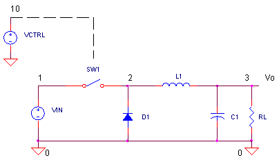
CIRCUIT

BUCK_BASIC.CIR Download the SPICE file
Switch-Mode Power Supplies (SMPS) deliver lot's of power while wasting very little. Why? SW1 delivers pulses of current to the output by being in one of two states - fully ON or fully OFF. Both of these states dissipate little power in SW1! And conserving power is what battery/portable design is all about. If you need an output voltage that's smaller than the input voltage, then the Buck Converter is your choice. There's just a handful of components. Their job is to transform the current pulses via SW1 into a constant voltage at the load. How? By looking at some voltage / current waveforms and playing with component values, you'll get a feel for each one's role and how to optimize performance.
BUCK BASICS
The Buck Converter is easy to understand if you look at the two main states of operation: SW1 ON and SW1 OFF.
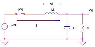
| ◄ SW1 is ON ► | L1 delivers current to the load | |
| With a voltage (Vin - Vo) across L1, current
rises linearly. How fast?
The rise (in amps per second) is determined by ΔI / ΔT = ( Vin - Vo) / L1 |

C1 smooths out L1's current changes into a stable voltage at Vo. Also, C1 is big enough such that Vo doesn't change significantly during one switching cycle. Where's D1? Its reversed biased and out of the picture for now.
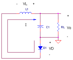
| ◄ SW1 is OFF ► | L1 maintains current to the load | |
|
As L1's magnetic field collapses, current
falls linearly through L1. How fast? The fall (amps per second) is again determined
by the voltage across L1 and its inductance. ΔI / ΔT = ( Vo + VD) / L1 |

Although L1's current direction is the same, what's happened to L1's voltage? It's reversed! That's L1 maintaining current flow by reversing its voltage when the applied voltage is removed. Also, check out what happens to D1 when the left end of L1 swings negative. Yes, it turns ON providing a path for L1's current to flow.
SWITCHING FREQUENCY
Given the components above, how do you control the exact output voltage? Typically, by using a Pulse-Width-Modulation (PWM) signal to drive SW1. This implies you need a pulse train that looks like this:
♦ A switching period of TS.
♦ An adjustable Pulse Width of TON (the time SW1 is ON)
Simply adjust the Duty Cycle (D = TON / TS) to get the output voltage you need!
At which frequency do you run this pulse train? Typically in the range of 10s to 100s of kHz. Why so high? There are two big benefits here:
1. As frequency goes up, parts usually get smaller, lighter and cheaper - very cool in portable design! You get a lot of power from a small volume of stuff. Or in other words - a high power density (W/in3).
2. The delay from input to output created by the switching time (Ts) becomes smaller.
So what's the big deal about delay? Later, when we place the Buck inside of a control loop, this delay can cause dreadful things to happen to the closed-loop response like overshoot, ringing or oscillation! Shorter cycle times (smaller delay times) - compared to the LC or controller response time - means less potential trouble when closing the loop.
THE SIMULATION CHALLENGE
Simulating switch-mode supplies can be fun, but challenging. Why? There are two time frames we interested in:
1) The short cycle-by-cycle period of the pulse train turning SW1 ON and OFF (micro seconds) .
2) The longer response of LC components as they respond to input or load changes (milli seconds)
As you can imagine, simulating the switching action may only require a few cycles. On the other hand, investigating the overall response may require simulating thousands of switching cycles.
FIRST SPICE RUN
Let's simulate the file BUCK_BASIC.CIR. VCTRL generates a pulse train of period TS = 20us and pulse-width TON = 5μs. When VCTRL is at 5V, SW1 drops to 0.01 Ω connecting 20V (VIN) to L1. When VCTRL is at 0V, SW1 pops open to 1 MΩ. effectively disconnecting VIN from L1. RL represents the load (analog/digital circuitry, motors, lights, etc.) powered by the Buck Converter.
CIRCUIT INSIGHT First we'll take a look at the longer overall response. Run a simulation and take a look at Vo by plotting V(3). How much overshoots happens due to the LC components? What voltage does output settle to? We might expect Vo to be related to VIN and D.
Vo = VIN ∙ D
= VIN ∙ ( TON / TS )
= 20 V ∙ ( 5 μs / 20 μs)
= 5 V
Add VCTRL to the plot by including trace V(10). Change its duty cycle by increasing or decreasing TON from 5 μs to values like 2.5, 10 or 15 μs. To do this, just change the 5US parameter in the PULSE definition of VCTRL. Does the above equation do a decent job of predicting Vo?
Finally, check out the current through L1 by opening a new plot window and adding trace I(L1). Awesome! See it rise and fall as SW1 turns ON and OFF (controlled by VCTRL). Let's take a closer look in the next section.
CYCLE BY CYCLE
We'd like to see a few cycles of the Buck Converter's operation, but here's the challenge: we want to see the simulation results after a few hundreds cycles, when the supply has settled to a steady state. How? Luckily, the Transient Analysis command comes with a handy feature that lets you throw away simulation results up to a specific delay time. For example, the statement
.TRAN 0.1US 840US 800US 0.1US
simulates the circuit to until 840 μs, but discards the data before 800 μs. Cool! The 40 μs saved represents two switching cycles for our viewing pleasure. Place an "*" in front of the original TRAN statement and remove the "*" from the new statement with the delay.
CIRCUIT INSIGHT Set TON to 5 μs and run a simulation of BUCK_BASIC.CIR. Plot Vo at V(3), VCTRL at V(10) and in a separate plot window, view the inductor current I(L1). Here we have wonderful view of I(L1) rising and falling as SW1 turns ON (VCTRL = 5 V) and SW1 turns OFF (VCTRL = 0 V).
Let's see the two different paths the inductor current takes as it rises and falls. Open a new plot window and add trace I(SW1). Wow, SW1's current is the same as L1's current, but only when SW1 is ON. Then it drops to 0 A. Sure, that makes sense as SW turns ON and OFF. Now add trace I(D1). Here D1's current is initially 0, then equals L1's current when D1 turns ON.
Finally take a look at the SW1's voltage at V(2). Basically we see VSW1 slammed to VIN = 20 V and then it drops to -0.3 V as D1 (Schottky diode) turns ON providing a pathway for L1's falling current.
INDUCTOR CURRENT
Does L1's current rise and fall as expected? Let's check by first calculating the rise rate of
ΔI / ΔT = ( Vin - Vo) / L1
= ( 20 V - 5 V ) / 50 μH
= 300,000 A/s
= 0.3 A/μs
Then calculate the total rise while SW1 is ON for 5 μs
ΔI = (Vin - Vo)/L1 ∙ ΔT
= 0.3 A/μs ∙ 5 μs
= 1.5 A
Now, check your SPICE plot. Does the current rise by approximately 1.5 A? (Actually, the rise might be a bit higher because Vo is slightly less than 5V.) You can also predict the fall rate by the equations above. What do you notice about the rise and fall of L1's current? Yes, they are equal! And this current change is appropriately named the inductor ripple current, ΔI.
What about the average inductor current, Iave? Find out by plotting AVG( I(L1) ). (If not using PSPICE, your simulator should have a similar function to plot the average of a variable.) Iave is important because this is the current that gets delivered to the load RL. What is the load current?
Io = Vo / RL ≈ 5 V / 5 Ω = 1 A
Does Iave match Io? Now, suppose the demand for Io increases. What happens to the ripple and average inductor current? Double Io by cutting RL from 5 Ω to 2.5 Ω. Rerun the simulation and check out ΔI and Iave? Iave doubles as expected! But notice - the ripple current ΔI remains the same! Why? Because Vin or Vo hasn't really changed. Next, we'll discover how the inductor ripple current plays a factor in the output ripple voltage.
OUTPUT VOLTAGE RIPPLE
Here's the big question on everyone's mind - especially the folks using the your supply: how much voltage ripple ΔVo rides on the output? Why ask? This ripple gets thrown on anything driven by Vo: IC's, transistors, voltage references, speakers, motors, etc. A large ΔVo could cause unexpected or poor behaviors for some components.
CIRCUIT INSIGHT Set TON = 5 μs and RL = 5 Ω. Run a simulation from 800 to 840 μs. Plot the output V(3) and inductor current I(L1) in separate windows. How big is ΔVo? There should be about 160 mVp-p riding on the output!
HANDS-ON DESIGN What if the design goal is less that 50 mVp-p of ripple? There's several options available for lowering the ripple. Return the components to their original values: L1 = 50 μH, C1 = 25 μF and RL = 5.
CAPACITOR - C1
Given an inductor ripple current, C1 has the lone responsibility for absorbing ΔI to minimize ΔVo. Try increasing C1 from 25 μF to a value like 50 or 100 μF. Has ΔVo reduced? Excellent! Side note - you might have to extend the simulation delay from 800 to 1000 μs. Why? A bigger C means a longer settling time for the LC combo.
INDUCTOR - L1
Let's lighten C1's burden of minimizing ΔVo by decreasing ΔI. The equation
ΔI = ( Vin - Vo)/L1 ∙ ΔT tells us that ΔI gets smaller as L1 gets bigger. With C1=25 μF, try increasing L1 from 50 μH to a value like 75 or 100 μH. Rerun the simulation. Did ΔVo shrink as expected?Cool, let's just put the mother of all inductors (and capacitors) in the circuit - thereby reducing ΔVo to nothing! Not so fast. Remember, larger values means bigger, bulkier and and more expensive components. Also keep in mind that big Ls and Cs slow down the supply's response time to input or load changes.
SWITCHING TIME - TS
The equation ΔI = ( Vin - Vo)/L1∙ΔT shows us another ripple reducing parameter - ΔT. If possible, reduce ΔT by choosing a shorter switching time Ts! Suppose you decreased Ts from 20 μs to 10 μs. To maintain Vo = TON/Ts∙Vin = 5V, change TON from 5 to 2.5 μs. To do this in SPICE, change the WIDTH and PERIOD parameters of the PULSE statement from
5US 20US to 2.5US 10US. Rerun the simulation with L1=50 μH and C1=25 μF. Has a smaller ΔT shrunk ΔI and consequently ΔVo?Okay faster is better - up to a point! Faster can mean more expensive components. Also, it takes a finite time to turn SW1 ON and OFF. During these times (ton, toff), SW1 dissipates a fair amount of power. Unfortunately, you can make Ts so small that ton and toff take up a significant portion of it. You end up wasting lots of power and your efficiency ends up in the basement.
CONTINUOUS VS. DISCONTINUOUS MODE
Up to now, we've seen current flowing continuously through L1. But there's a mode were the current goes to zero during the last portion of the switching cycle.
Continuous Mode (2 states of L1)
1) Current rises with SW1 ON.
2) Current falls with SW1 OFF.Discontinuous mode (3 states of L1)
1) Current rises with SW1 ON.
2) Current falls with SW1 OFF.
3) Current goes to 0 A with SW1 OFF.
How does L1's current go to zero? Let's find out.
CIRCUIT INSIGHT Set TON = 5 μs, TS = 20 μs and RL = 5 Ω. Run a SPICE simulation and plot the output V(3) and inductor current I(L1) in separate windows. We see ΔI riding on top of Iave = 1A. Now reduce the load by raising RL to 10 Ω. Rerun the circuit. A couple of interesting things here. First, L1's falling current drops to 0A! Why? Iave is not big enough to keep ΔI above 0 A. And second, Vo has risen significantly. Question: does Vo = VIN∙( TON/TS ) still hold in discontinuous mode? Raise RL to 20 Ω and vary TON to find out.
CIRCUIT INSIGHT Let's look at SW1's voltage VSW1. Set TON = 5 μs, TS = 20 μs, RL = 5 Ω, and run SPICE simulation. Plot SW1's voltage V(2) and inductor current I(L1). As before, we see VSW1 swing to 20 V with SW1 ON and then swing back to -0.3 V as D1 turns ON providing a pathway for L1s falling current.
But now raise RL to 10 Ω and rerun the circuit. Wow! What's happening to VSW1 when L1's current goes to zero and D1 turns OFF? You've got some major ringing here. Why? With D1 and SW1 OFF you'd expect a high impedance at one end of L1. However, D1 presents some parasitic capacitance to the circuit. And when this capacitance sees L1, they hit the dance floor and ring until SW1 turns ON again. (SW1 also presents some parasitic capacitance not modeled here.)
DESIGN TIME Typically, application notes recommend running your supply in continuous mode for your expected loads. Why? You get big benefits when optimizing a Buck converter inside of a control loop.
- First, the gain is stable. In continuous mode, Vo is approximately set by VIN and D only, regardless of load or other component values. In discontinuous mode, Vo depends on VIN, D, L1, RL and Ts.
- Second, for continuous and discontinuous modes, the frequency responses are different. You can spend time tuning the control loop for a good transient response in continuous only to see it change in discontinuous mode.
For a given load, how do you place your supply in continuous mode? Increase L1 until ΔI is small enough compared to Iave to keep the current above zero during the entire cycle. However, some applications can have a wide range of load conditions where entering discontinuous mode may be unavoidable.
CAPACITOR ESR
Up to now, C1 has successfully reduced ΔVo. But real capacitors behave as if there's a small resistor in series with its capacitance - the Equivalent Series Resistance (ESR). Change the C1 statement to two statements.
C1 3 4 25UF
RC1 4 0 0.5
RC1 = 0.5 Ω models the ESR of C1. With L1 = 50 μH, C1 = 25 μF and RL = 5, we saw ΔVo = 160 mVp-p. Will adding ESR have an effect on ΔVo?
CIRCUIT INSIGHT Run a simulation and plot the V(3) and I(L1) in separate windows. How big is ΔVo? Wow, the output ripple is horrible. Why? The inductor ripple ΔI, normally absorbed by C1, flows right through the ESR adding to the voltage ripple! Can we predict the ripple from ESR?
ΔVo = ΔI ∙ ESR = 1.5 A ∙ 0.5 = 0.75 V
HANDS-ON DESIGN Okay let's crank up C1 to 50 or 100μF and rerun the simulation. Unfortunately, no progress here - C1 just looks like more of a short circuit to the ESR. What other options do you have? Basically, you need to reduce ΔI, ESR or both. Try increasing L1 to 100μH to knock down ΔI. Any improvement? Suppose you buy better capacitor with a lower ESR. Reduce RC1 to 0.2 or 0.1 Ω. How much of ΔVo remains? Okay, trying reducing ΔI by picking a higher switching frequency (smaller Ts) to squash ΔVo.
FINAL NOTES
If you made it this far - high fives for you! Hopefully, by experimenting with component values, you've got a good feel for switch-mode power supplies. The only way to learn the river's rapids is to launch the kayak and start paddling. We've got more thrills ahead - closing the Buck converter inside of a control tool! And we'll measure and optimize efficiency in upcoming topics.
SIMULATION NOTES
Check out Voltage Control Mode
to see how the feedback loop is closed.
The
Buck Converter AC Model
helps you create an AC SPICE model.
Tuning a Buck Converter lets you compensate
a converter for minimum overshoot and ringing.
Find out where power gets lost in the topic
Buck Converter Power Loss.
SPICE FILE
Download the file or copy this netlist into a text file with the *.cir extension.
BUCK_BASIC.CIR - BASIC BUCK CONVERTER
*
* SWITCH DRIVER
VCTRL	10	0	PULSE(0V 5V 0 0.01US 0.01US 5US 20US)
R10	10	0	1MEG
*
* INPUT VOLTAGE
VIN	1	0	DC	20
*
* CONVERTER
SW1	1 2	10 0 	SW
D1	0	2	DSCH
L1	2	3	50UH
C1	3	0	25UF
*
* LOAD
RL	3	0	5
*
*
.MODEL	SW	VSWITCH(VON=5V VOFF=0V RON=0.01 ROFF=1MEG)
.MODEL DSCH D( IS=0.0002 RS=0.05 CJO=5e-10  )
*
* ANALYSIS
.TRAN 	1US  	800US
*.TRAN 	0.1US  	840US  800US 0.1US
*
* VIEW RESULTS
.PLOT	TRAN	V(2) V(3)
.PROBE
.END
© 2005 eCircuit Center