SMPS - POWER LOSS
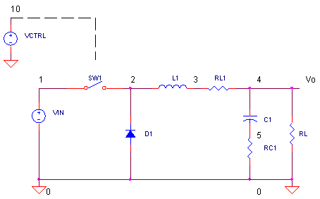
CIRCUIT
BUCK_PWR1.CIR Download the SPICE file
What is the main goal as a designer of Switch-Mode Power Supplies (SMPS)? You need deliver power from an input source to your load. But the key is avoiding loss of precious power during delivery, especially in battery powered devices. To this end, you've got to know: 1) which components are your power wasters and 2) how to minimize it. We'll look at the instantaneous power dissipated in each component. In a later topic, we'll evaluate the supply's power efficiency by comparing the average power output versus average power input.
WHERE DOES THE POWER GO?
While most of the power in an SMPS goes to the load, some gets stolen away. How? Resistive and semiconductor elements convert power into heat. What about inductors and capacitors? Strictly speaking, reactive components store energy only. However, real world components have parasitic elements modeled as resistance in series with the reactance. Let's look at the power robbers in the buck converter.
| Power Dissipating Element | Comment | Plotting Instantaneous Power in SPICE | |
| SW1 |
Power loss while SW1 is ON and current
flows through L1. Power loss while transitioning between OFF and ON states. |
V(1,2)*I(SW1) | |
| RL1 | Power loss in the equivalent series resistance of inductor L1. | V(3,4)*I(RL1) | |
| RC1 | Power loss in the equivalent series resistance (ESR) of capacitor C1. | V(5)*I(RC1) | |
| D1 | Power loss while SW1 is OFF and D1 provides a path for L1's current. | V(0,2)*I(D1) |
What does instantaneous power look like? It varies depending on the component and the point in the switching cycle. (Ultimately, we're interested in measuring the average power over one switching cycle.)
BASIC BUCK
In a previous topic, we got our first view of the Buck Converter . This switching supply runs at 50 kHz (Ts = 20 μs). With Ton = 8.33 μs for SW1, the input 12 V gets converted to an output of
Vo = D ∙ Vin
= Ton / Ts ∙ Vin
= 8.33 μs / 20 μs ∙ 12 V = 5V
Let's take out the buck for a run. We'll look at just one cycle (20 μs) of operation after a 1000 μs delay allowing the supply to settle.
CIRCUIT INSIGHT Run a SPICE simulation of the file BUCK_EFF.CIR. Plot the output at V(4). You should see about Vo = 5 V with some ripple ΔVo = 300 mVp-p.
SW1 POWER
How much power gets lost in SW1 and how can we minimize it? Open another plot window and add a trace representing the SW1's instantaneous power: V(1,2)*I(SW1). The plot shows units of Volts, but we know it represents Watts. (NOTE: Although SW1 is typically a MOSFET, for simplicity its modeled here using a voltage controlled switch.)
SWITCHING TIMES There's a couple of interesting regions here. First, notice the large power spikes! Where do they come from? We know that an analog switch has two low power modes - fully-ON (low R) and fully OFF (high R). But what happens when the switch transitions between these two states. Its in these mid-values of R (high current, medium resistance) that lots of power get dissipated.
HANDS-ON DESIGN Try reducing the transition time between ON and OFF states. You can do this by decreasing trise and tfall parameters from 1 μs to 0.5 or 0.1 μs in the PULSE statement of VCTRL.
VCTRL 10 0 PULSE(0V 5V 0 0.5US 0.5US 8.333US 20US)
Because the analog switch SW1 is controlled by VCTRL, reducing trise / tfall simulates selecting a MOSFET with a faster switching time. Rerun the SPICE file. What happened to the power spikes? Hopefully, they got narrower. And narrower means a smaller average power over one cycle!
ON RESISTANCE Another interesting region is where the switch is ON. This is where SW1 passes current to L1. How much power is dissipated here? Run a cursor over this region. Can we lower the power lost? Try a MOSFET with a lower RON. You can simulate this by reducing RON in the SW1 definition from 0.2 Ω to 0.1 Ω or lower.
.MODEL SWP VSWITCH(VON=5V VOFF=0V RON=0.1 ROFF=1MEG)
Rerun the SPICE simulation. Fantastic! You've successfully reduced the power spent in SW1. Can we do the same with the other components?
INDUCTOR AND CAPACITOR POWER
A significant amount of current flows through L1 and C1. Unfortunately,
their series resistances, RL1 and RC1, convert precious power to useless
heat. Open another plot window and add the traces
V(3,4)*I(RL1) and
V(5)*I(RC1).
HANDS-ON DESIGN No doubt, there's energy waste going on here! What to do? Try choosing inductor and capacitors with lower equivalent series resistance. You can simulate this by decreasing RL1 or RC1 by a factor of 2 or 4. Run a new simulation. A smashing success! Now trim a little heat from the other component.
NOTES: 1) There's limits to the lowest equivalent series resistance that can be manufactured. 2) Sometimes a capacitor with too small of an ESR can cause stability problems when placing the switcher inside of a control loop. 3) There's some power lost in the inductor's core not modeled here.
D1 POWER
Lastly, we arrive at one of the top power wasters - the big free-wheelin' heat radiatin' diode D1. Although, this Schottky diode has a
lower on voltage (0.3 V) compared with its cousin the silicon diode (0.7 V),
power loss is still significant. Open another plot window and add the
trace
V(0,2)*I(D1). You
might want to adjust the y-axis limits to 0 and 1.
HANDS-ON DESIGN What happens during the cycle where SW1 turns off and all of L1's current flows through D1? Run a cursor over the trace to see the power given up. This is bad! Especially because a diode with a lower on voltage isn't available. But how can we lower the voltage?
SYNCHRONOUS CONVERTER D1 acts as automatic switch providing a current path for L1 when SW1 switches OFF. But what if we replaced D1 with an actual switch!
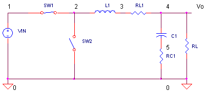
Why? SW2's low on resistance - and therefore low on voltage - could reduce power loss during this part of the switching cycle. Remove D1 by adding a "*" before its statement. Add SW2 by removing the "*" before its statement. The models for SW1 and SW2 look like this.
.MODEL SWP VSWITCH(VON=5V VOFF=0V RON=0.2 ROFF=1MEG)
.MODEL SWN VSWITCH(VON=0V VOFF=5V RON=0.2 ROFF=1MEG)
The major difference here being SW2 turns ON when SW1 turns OFF. Run a new simulation, remove the trace for D1's power and add a trace for SW2's power V(2)*I(SW2). The power should be lower than with D1. If not, choose a switch with a lower RON by lowering this parameter in the SWN model.
Adding a switch changes the supply's name to a synchronous converter. Although it has more complexity, some battery powered applications may require it.
SIMULATION NOTES
Understand the basic operation of the
Buck Converter.
Check out Voltage Control Mode
to see how the feedback loop is closed.
The
Buck Converter AC Model
helps you create an AC SPICE model.
Tuning a Buck Converter lets you compensate
a converter for minimum overshoot and ringing.
SPICE FILE
Download the file or copy this netlist into a text file with the *.cir extension.
BUCK_PWR1.CIR - BUCK CONVERTER POWER LOSS
*
* SWITCH DRIVER
VCTRL	10	0	PULSE(0V 5V 0 1US 1US 8.333US 20US)
R10	10	0	1MEG
*
* INPUT VOLTAGE
VIN	1	0	DC	12
*
* BUCK CONVERTER
SW1	1 2	10 0 	SWP
*SW2	2 0	10 0	SWN
D1	0	2	DSCH
L1	2	3	100UH
RL1	3	4	0.1
C1	4	5	50UF
RC1	5	0	0.5
*
* LOAD
RL	4	0	5
*
*
.MODEL	SWP	VSWITCH(VON=5V VOFF=0V RON=0.2 ROFF=1MEG)
.MODEL	SWN	VSWITCH(VON=0V VOFF=5V RON=0.2 ROFF=1MEG)
.MODEL DSCH D( IS=0.0002 RS=0.05 CJO=5e-10  )
*
* ANALYSIS
.TRAN 	0.1US  	1020US  1000US 0.1US  UIC
*
* VIEW RESULTS
.PLOT	TRAN	V(1) V(4)
.PROBE
.END
© 2005 eCircuit Center