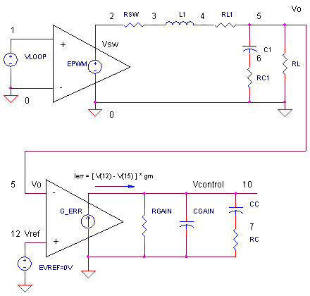
BUCK CONVERTER - AC MODEL
CIRCUIT
BUCK_VM_OL.CIR Download the SPICE file
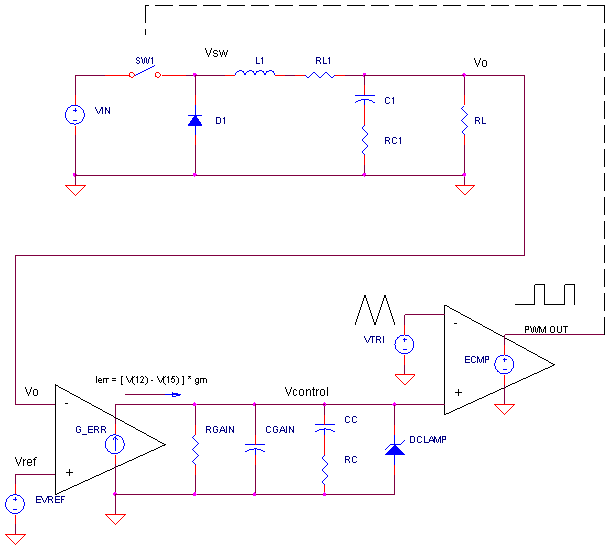
We've already developed a SPICE model for the Buck Converter in a voltage control loop. The controller performed brilliantly holding the output steady under varying load conditions. However, closing the loop is fraught with danger! Without proper insight, Vo can start ringing and oscillating out of control! And what is this insight? By looking at the AC frequency response of a control circuit with its loop opened (also called the Bode plot), you can predict and tame potentially wild behavior. Many of the Buck's components are linear - they work as well in the frequency domain as they do in the time domain. But some non-linear components need a linear transformation before moving to the frequency domain.
STARTING POINT
To generate an AC model, we begin with the time-response circuit.
Calculating frequency response assumes you're working with linear
components. Cool! Many parts in the Buck Converter get a free pass right to
the AC Model.
L1, RL1, C1, RC1, RL, GERR, etc.
Unfortunately, non-linear
components must be first transformed into their small-signal linear equivalents.
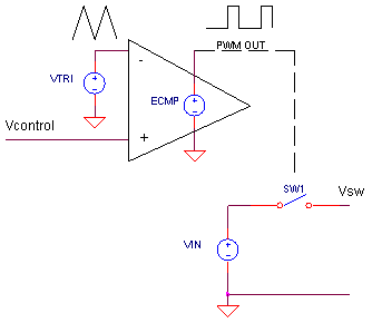
SW1, D1, ECMP
PWM, VIN and SW1 - AC MODEL
Our challenge is to take the following non-linear PWM circuit and find its linear equivalent.
We’ll model this circuit with Vcontrol as the input and Vsw as the output. Linearizing a circuit means finding its time-averaged equivalent behavior. How? We can predict the average value of Vsw over one switching-cycle time as a function of Vcontrol. (Assume the source voltage is constant VIN = 12 V and the triangle wave VTRI = 0 to 5 V.)
|
Vcontrol (Input) |
Duty Cycle |
Vsw_ave (Output) |
|
| 0.0 V | 0 % | 0 V | |
| 2.5 V | 50 % | 6 V | |
| 5.0 V | 100 % | 12 V |
With this information, we can write a simple gain formula
K_pwm = ΔVsw_ave / ΔVcontrol
= 12 V / 5 V
= 2.4 V/V
In SPICE, the PWM, VIN and SW1 distills down to a Voltage-Controlled
Voltage Source (VCCS) with a gain of 2.4 V/V.
EPWM
2 0 1 0 2.4
Although its a simple AC model, I've seen several application notes use it successfully to model a Buck converter. More accurate models can be derived using state-space averaging techniques.
OPEN LOOP AC RESPONSE
Now that we've got our AC models, let's find the frequency (AC) response of the open-loop gain. Why? The gain and phase of the open loop provide critical insight how to compensate a control loop (Next topic). How do we open the loop? Pick a point to open the circuit such as where Vcontrol connects to ECMP of the PWM. Then connect an AC test source (VLOOP) to the point where the loop was opened (see circuit at top of page). Notice in the closed-loop version, node 10 would be connected to node 1.
Here's a guided tour of interesting features you might see in the open-loop frequency response. In general, negative phase pushes a circuit towards instability (ringing and oscillations); positive phase improves stability.
| frequency | (Hz) | comment | |
| fLC = 1 / ( 2∙π∙√ L1∙ C1) | 1.59 kHz | Low-pass cutoff frequency of 2-Pole LC filter. Response falls at - 40dB/decade above cutoff. Adds -180 deg of phase. | |
| fESR = 1 / ( 2∙π∙RC1∙C1) | 7.96 kHz | Zero created by C1 and its own Equivalent Series Resistance RC1. Adds +90 deg of phase. | |
| fPOLE = 1 / ( 2∙π∙RGAIN∙CC) | 1.59 Hz | Low-pass cutoff (pole) created by compensation capacitor CC and the gain resistor RGAIN. Adds -90 deg of phase. | |
| fZERO = 1 / ( 2∙π∙RCC∙CC) | 398 Hz | High-pass cutoff (zero) created by compensation pair CC and RC. Adds +90 deg of phase. |
LC FILTER RESPONSE
Let's take a look at the frequency response at the output of the LC filter. Later, we'll plot the error amp/compensation section.
CIRCUIT INSIGHT
Run an AC Analysis of the SPICE file BUCK_VM_OL.CIR. Plot the
magnitude (dB) at the output of the LC circuit by adding trace DB(V(5)).
Open another plot window and plot the phase VP(5). Here's your basic 2-pole
low-pass response. A slight peak at the cutoff frequency while the phase
swings to
-180 at the same frequency. Not good for stability! But what happens at
higher frequencies. Yes, the phase swings in the positive direction. Why?
Its the zero created by capacitor C1 and its ESR component RC1. Suppose you
selected C1 with a lower ESR. Reduce RC1 and rerun the simulation. The zero
moves to higher frequency and so does the point where the positive phase
kicks in.
ERROR AMP/COMPENSATOR RESPONSE
CIRCUIT INSIGHT Rerun an AC Analysis of BUCK_VM_OL.CIR. Plot the magnitude and phase of the error amp/compensator only by plotting DB(V10))-DB(V(5)) and VP(10)-VP(5)-180 in separate windows. (We've included -180 to remove the effect of G_ERR's negative input on the plot.) You should see a pole (low-pass cutoff) at 1.59Hz and a zero (high-pass cutoff) at 398 Hz that counteracts the pole.
What good is the pole created by RGAIN and CC? To stabilize a control loop, the pole reduces the gain at higher frequencies where the phase can get unpredictable. Why? Uncontrolled parasitic capacitances create poles (more negative phase) in unexpected places. The pole reduces gain to a small value before the phase trouble can begin. The bad news is that the RGAIN/CC pole adds its own -90 degrees to the mix - also bad for stability. What's the fix? A zero to the rescue! RC and CC create a zero adding positive phase ultimately bringing the total phase back to 0 deg.
Vary RC to values like 20 kΩ or 20 Ω and rerun the simulation. Vary CC up and down. Check out how the pole and zero shifts with each change.
TOTAL FREQUENCY RESPONSE
CIRCUIT INSIGHT Okay, now let's see the whole open-loop frequency response (Bode plot). Rerun an AC analysis with RC = 2k and CC = 0.2 uF. Plot the magnitude and phase (in separate windows) of the total circuit: DB(V(10)) and VP(10). Wow, what a mess at first glance! But it does provide a picture of the stability story. Here's the main point of interest:
Find where the magnitude falls to 1 ( 0 dB)
► A phase near 0 deg (or 360 deg) reveals a circuit response that rings.
► A phase at 0 deg indicates a circuit that oscillates!
How does our AC response look? Not too bad - at 0dB we're about 40 deg away from 0 deg. A reasonable safety margin. Try changing RC or CC. What happens to the safety margin?
Return the values to RC = 2 kΩ and CC = 0.2 uF. What happens if you purchase a better capacitor C1 with a lower ESR. Simulate this by lowering RC1 to 0.01 Ω. What happened?!!! The safety margin of phase actually got worse because the C1/RC1 zero gets moved to a higher frequency. Yes, a lower ESR means lower output ripple, but it also can degrade stability.
Next topic we'll compensate the converter by adjusting RC and CC in the frequency domain. Then, we'll see their effect in the time domain.
SIMULATION NOTES
Understand the basic operation of the
Buck Converter.
Check out Voltage Control Mode
to see how the feedback loop is closed.
Tuning a Buck Converter lets you compensate
a converter for minimum overshoot and ringing.
Find out where SMPS power gets lost in the topic
Buck Converter Power Loss.
SPICE FILE
Download the file or copy this netlist into a text file with the *.cir extension.
BUCK_VM_OL.CIR - BUCK CONVERTER AC MODEL
* OPEN-LOOP FREQUENCY (AC) ANALYSIS
*
* INPUT VOLTAGE
VLOOP	1	0	AC	1
R1	1	0	1MEG
*
* AC PWM
EPWM	2 0	1 0	2.4
RSW	2	3	0.1
*
L1	3	4	50UH
RL1 4	5	0.01
C1	5	6	200UF
RC1	6	0	0.1
*
* LOAD
RL	5	0	5
*
* ERROR AMP AND COMPENSATION
GERR	0 10	12 5	0.002
RGAIN	10	0	500K
CGAIN	10	0	10PF
CC	10	7	0.2UF
RC	7	0	2000
*
VREF	12	0	DC 0
*
* ANALYSIS
.AC DEC 20 0.1HZ 1MEGHZ
*
* VIEW RESULTS
.PLOT	AC V(10)
.PROBE
.END
© 2006 eCircuit Center