BUCK CONVERTER
FREQUENCY COMPENSATION
CIRCUIT
BUCK_COMP.CIR Download the SPICE file
You can tell it's time to compensate a switch-mode power supply. Beads of sweat form on your brow. You reach for a handful of R and C components. You strain to remember some control theory you read long ago. I should know, it happens to me every time. But then you dive in, you struggle, and eventually - out of the ringing and oscillations - comes a response that begins to look normal. This topic pulls together a series of SMPS adventures - the Buck Converter - Voltage Control Mode, and the Buck Converter - AC Model - with frequency compensation as the final topic.
TUNING MISSION
Basically your mission is to adjust CC and RC for the following desirable
behavior.
In the time domain (Transient Analysis),
the circuit response should look like this:
1. A quick response response when the load changes.
2. A minimum of ringing and overshoot.
In the frequency domain (AC Analysis), the corresponding open-loop response should look like this:
1. A high bandwidth, f_0dB. Bandwidth is defined as the frequency where the magnitude falls to 0dB (unity gain).
2. A phase that's far away from 0 deg (or ± 360 deg) at f_0dB.
Many application notes suggest a maximum open-loop bandwidth of 1/5 the switching frequency to avoid oscillation. For this circuit that means a max bandwidth of f_0dB = 100 kHz / 5 = 20 kHz.
CLOSED-LOOP - TRANSIENT ANALYSIS
The feedback loop is closed around this Buck Converter using Voltage Mode Control. Basically, that means we regulate the output by adjusting the input voltage to the LC filter. Check out Voltage Control Mode for a tour. Here's a quick summary of the converter
Vin = 12 V
Vo = 5 V
fs = 100 kHz
L1 = 100 μH
C1 = 200 μF
ESR of C1 = 0.1 ΩError Amp Gain = 2000 V/V
PWM Gain = 0 to 5V input , 0 to 100% Duty Cycle (0 to 12 V) Output
OPEN-LOOP - AC ANALYSIS
Here's the AC model you can use to view the magnitude (in dB) and phase of the open-loop response (together called the Bode plot). This AC view helps you predict the time response under closed-loop conditions. How was the SPICE model developed? Check out the Buck Converter AC Model.
BUCK_COMP_OL.CIR Download the SPICE file
Repeated here is a guided tour of interesting features you'll see in the open-loop frequency response. In general, negative phase pushes a circuit towards instability (ringing and oscillations); positive phase improves stability. Don't forget! The negative input of the error amp adds -180 deg of phase before you even start adding the other contributors.
| frequency | (Hz) | comment | |
| fLC = 1 / ( 2∙π∙√ L1∙ C1) | 1.59 kHz | Low-pass cutoff frequency of 2-Pole LC filter. Response falls at - 40dB/decade above cutoff. Adds -180 deg of phase. | |
| fESR = 1 / ( 2∙π∙RC1∙C1) | 7.96 kHz | Zero created by C1 and its own Equivalent Series Resistance RC1. Adds +90 deg of phase. | |
| fPOLE = 1 / ( 2∙π∙RGAIN∙CC) | TBD | Low-pass cutoff (pole) created by compensation capacitor CC and the gain resistor RGAIN. Adds -90 deg of phase. | |
| fZERO = 1 / ( 2∙π∙RC∙CC) | TBD | High-pass cutoff (zero) created by compensation pair CC and RC. Adds +90 deg of phase. |
TUNING THE BUCK
Here's one approach for tuning the Buck converter. Pick a capacitor value for CC (the IC manufacturer will usually suggest one) and then adjust RC to meet your tuning goals. Let's start with CC = 47 nF and RC = 0 Ω. Then begin increasing RC.
HANDS-ON DESIGN For each set of values for RC and CC:
1. Run an AC Analysis of BUCK_COMP_OL.CIR to check the bandwidth and stability conditions. Plot the magnitude DB(V(10)) and phase VP(10) in separate windows
2. Then run a Transient Analysis BUCK_COMP.CIR to check the recovery time and ringing in response to a load change. Plot the output voltage V(15) and the output current I(RSENSE) in separate windows
Repeat the above simulations for each new value of CC and RC.
CC = 47 nF and RC = 0 Ω
Open-Loop AC Response
Set CC = 47 nF and RC = 0.2 ohms (close enough to zero) and run an AC Analysis of BUCK_COMP_OL.CIR. What is the bandwidth (f_0dB) of DB(V(10))? Looks like about 4 kHz. How does the phase behave near f_0dB? Yes, the phase goes dangerously beyond 0 deg and back again. Why? Negative feedback contributes
-180 deg, the LC filter another -180 deg and the CC/RGAIN pole another -90 deg. The only positive phase contributor is C1 and its ESR (RC1) adding +90 deg. This total phase of -360 deg (or 0 deg) places us right in oscillation country.Closed-Loop Transient Response
Run a Transient Analysis of BUCK_COMP.CIR. What 's happening? Yes, the output V(15) oscillates wildly. In its present state, this power supply is a useless pile of heat generating components
CC = 47 nF and RC = 2 kΩ
Open-Loop AC Response
Pick a value of RC around 2 kΩ and run BUCK_COMP_OL.CIR. Where is the 0 dB crossing now? Good news, f_0dB moved higher. What about the phase? More good news - first the phase dips near 0 deg, but then it moves more positive at f_0dB. Why? The zero created by RC and CC adds +90 deg for a total phase of about +45 deg at f_0dB! We're moving in a more stable direction.
Closed-Loop Transient Response
Run BUCK_COMP.CIR with RC = 2 kΩ. How does the output V(15) look now? The Buck appears to be regulating Vo to 5V! But before we break open the bubbly, how well does it handle a load change? Change the Y axis voltage range to 4.9 V and 5.1 V. Notice the overshoot and ringing as the load changes from 0.5 to 1.0 A. The ringing period should correspond to the 0 dB frequency ( tRING = 1 / f_0dB ) of the open-loop AC response - control theory in action! Can we do a better job of tuning?
CC = 47 nF and RC = 10 kΩ
Open-Loop AC Response
Try increasing RC to 10 k and check the AC Response. You'll notice the phase never gets near 0 deg! And even better, the phase at f_0 dB increases to about +90 deg. The only danger here is that f_0dB gets close to 20 kHz, the upper recommended limit of bandwidth (see above).
Closed-Loop Transient Response
The Transient Response at V(15) shows a quick recovery to a load change with almost no ringing.
HANDS-ON DESIGN Try a different starting value for value for CC like 10 nF or 100 nF. Then simulate the circuit for a series of values for RC starting at 0 ohms. Do the ringing and oscillation frequencies change? What's the effect on recovery time?
SIMULATION NOTE When a I tried a real Buck converter on the bench, the behavior was very similar to the simulations. Way cool! However, for higher values of RC (>> 10 kΩ), the converter started oscillating. The bad news? Neither the AC nor Transient simulations predicted this instability. It shows the limitations of this relatively simple SPICE model. More complex models are available. Still, this one carried us nicely through some basic operation, design and tuning of the Buck Converter
LOW ESR
Although a lower ESR for C1 reduces output ripple, it can actually have a bad effect on stability. Why? C1 and its ESR (RC1) add a zero ( fz = 1/(2π ∙ C1 ∙ RC1 ) to the open loop response. This adds +90 degrees to the open loop which is good for stability. However, by making RC1 smaller, fz gets pushed to a higher frequency. This means the added +90 deg gets moved to a higher frequency too. Unfortunately, f_0dB occurs at a lower frequency where the +90 deg is needed the most.
CIRCUIT INSIGHT With CC = 47 nF and RC = 2000 Ω, reduce RC1 from 0.1 Ω down to 0.05 or 0.02 Ω. What happens in the frequency domain? The Bode plot does predict a pretty story in the time domain. The phase looms near 0 deg at f_0dB. Now try the closed loop time response. Does the response ring more severely as predicted? So what's the fix? A more complex compensation network may be needed to handle this situation. Or, select C1 with higher ESR if the higher output ripple is acceptable.
SIMULATION NOTES
Understand the basic operation of the
Buck Converter.
Check out Voltage Control Mode
to see how the feedback loop is closed.
The
Buck Converter AC Model
helps you create an AC SPICE model.
Find out where SMPS power gets wasted in the topic
Buck Converter Power Loss.
SPICE FILE
Download the file or copy this netlist into a text file with the *.cir extension.
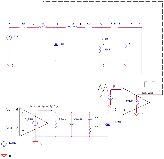
BUCK_COMP.CIR - BUCK CONVERTER - VOLTAGE MODE CONTROL
* FREQUENCY COMPENSATION
*
* INPUT VOLTAGE
VS	1	0	DC	12
RS	1	2	0.1
*
* BASIC BUCK TOPOLOGY
S1	2 3	11 0 	SW
D1	0	3	DSCH
L1	3	4	100UH
RL1 4	5	0.2
C1	5	6	200UF
RC1	6	0	0.1
* MEASURE TOTAL CURRENT OUT W/ RSENSE
RSENSE	5	15	0.01
*
* LOAD
RL	15	0	10
* PULSED LOAD
ILOAD 15 0 PWL(0US 0A  1000US 0A  1001US 0.5A  1500US 0.5A  1501US 0A  2000US 0A)
*
* VOLTAGE MODE CONTROL
* REFERENCE VOLTAGE
VREF	12	0	PWL(0US 0V  10US 0V   201US 5V  1000US 5V)
*
* ERROR AMP AND COMPENSATION
G_ERR	0 10	12 15	0.005
RGAIN	10	0	400K
CGAIN	10	0	5PF
CC	10	7	47NF
RC	7	0	.2
DCLAMP	0	10	DZ45
*
* TRIANGLE WAVE FOR PWM
* (PULSE SOURCE WITH LONG RISE/FALL TIMES)
VTRI	9	0	PULSE(0V 5V 0 4.9US 4.9US 0.1US 10US)
R9	9	0	1MEG
*
* PWM COMPARATOR
ECMP	11	0	TABLE {V(10,9)} = (-5MV 0V) (5MV, 5V)
R11	11	0	1MEG
*
*
.MODEL	SW	VSWITCH(VON=5V VOFF=0V RON=0.1 ROFF=100K)
.model	DZ45	D( BV=4.5 )
.MODEL DSCH D( IS=0.0002 RS=0.05 CJO=5e-10  )
*
* ANALYSIS
.OPTIONS ABSTOL=1M RELTOL=1M ITL5=0
.TRAN 	1US  	2000US 0US  1US
*
* VIEW RESULTS
.PRINT	TRAN	V(1) V(15)
.PROBE
.END
Download the file or copy this netlist into a text file with the *.cir extension.
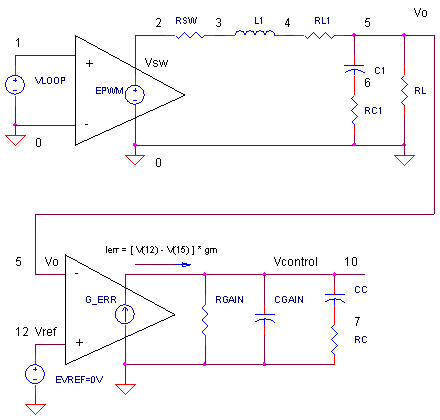
BUCK_COMP_OL.CIR - BUCK CONVERTER - VOLTAGE MODE CONTROL
* FREQUENCY COMPENSATION
* OPEN-LOOP FREQUENCY (AC) ANALYSIS
*
* INPUT VOLTAGE
VLOOP	1	0	AC	1
R1	1	0	1MEG
*
* AC PWM
EPWM	2 0	1 0	2.4
RSW	2	3	0.1
*
L1	3	4	100UH
RL1 4	5	0.2
C1	5	6	200UF
RC1	6	0	0.1
*
* LOAD
RL	5	0	10
*
* ERROR AMP AND COMPENSATION
GERR	0 10	12 5	0.005
RGAIN	10	0	400K
CGAIN	10	0	5PF
CC	10	7	47NF
RC	7	0	.2
*
VREF	12	0	DC 0
*
* ANALYSIS
.AC DEC 20 0.1HZ 1MEGHZ
*
* VIEW RESULTS
.PLOT	AC V(10)
.PROBE
.END
© 2006 eCircuit Center