Advanced Audio Amplifier
CIRCUIT
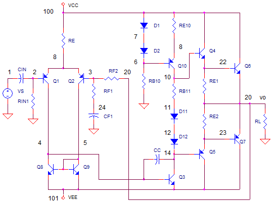
ADVANCED_AMPLIFIER.CIR Download the SPICE file
It all started with the Basic Audio Amplifier. This is roughly the minimum number of components that represents the classic audio amplifier topology. You can clearly see the three stages found in many audio amps (and op amps today). However, looking at actual audio designs, you'll find the basic topology has been tweaked and enhanced in a few key locations.
We've already covered many of the modifications to each stage individually. But, this is where we put it all together into the advanced audio amplifier.
THE IMPROVEMENTS
Here's a quick tour of design improvements of the audio amplifier. There's an enhancement for each of the three stages: Differential, Voltage Gain, Output Buffer. Why bother messing with the design? Higher gain and better output drive lead to a lower distortion performance. Click on the links below to find out more.
| Current Mirror | The Current Mirror (Q8,Q9) doubles the gain of your differential amplifier. It also balances the current in each transistor (Q1, Q2) nicely. Both high gain and balancing helps lower the overall distortion. | |
| Active Load | Replacing the collector resistor of the gain stage (Q3) with an Active Load (Q10) raises the voltage gain and provides better current drive to the positive half of the output buffer. | |
|
Darlington Output
|
Driving a low impedance like 8 ohms demands a lot of current from the output buffer. A Darlington Output Buffer helps deliver the current and minimize the load on the gain stage. This keeps the overall gain high and the distortion low. |
AMPLIFIER ANALYSIS
Let's step through a simple audio amp with a signal gain of 10 V/V (20 dB). We'll run it from a +/- 15V supply.
► Advanced Audio Amplifier
► DC BIAS
First, what is the bias current of Q1 and Q2? The current through RE splits into Q1 and Q2, so we calculate
Ic1 = Ic2 = 1/2 Ibias
= 1/2 (VCC - VbeQ1) / RE = 1/2 (15 - 0.7) / 14.3k = 0.5 mA► DIFFERENTIAL INPUT SIGNAL GAIN
The transconductance of Q1 and Q2 is gm = Ic1 / VT = 0.5 mA / 26mV = 0.0192 (A/V). The transconductance of the input stage, gm1 = Ib(Q3)/V(2,3), is double to that of the basic amplifier (1/2*gm) thanks to the current doubling of the current mirror Q8, Q9.
gm1 = 2* (1/2* gm) = gm = 0.0192 (A/V)
► CLOSED-LOOP GAIN
The feedback resistors (RF1, RF2) determine the close-loop signal gain from input (V2) to output (V20).
Acl = RF2 / RF1 +1 = 9k / 1k + 1 = 10 (V/V)
► AC SMALL-SIGNAL BANDWIDTH
The unity gain bandwidth of the open-loop amplifier is determined by gm1 and CC.
fu = gm1 / ( 2 pi CC) = 0.0192 / ( 2 pi 500 pF) = 6.12 MHz
The bandwidth of the closed gain amplifier is simply
fc = fu / Acl = 6.12 MHz / 10 V/V = 612 kHz
The low frequency bandwidth is set by one of two high pass filter cutoff frequencies, which ever is higher
fhp1 = 1 / ( 2 pi CIN * RIN) = 15.9 Hz
fhp2 = 1 / ( 2 pi RF1 * CF1) = 15.9 Hz
► SLEW-RATE
Finally, for big input signals, how fast can the output change? It's determined by the max current available Ibias in the differential amplifier and CC.
Slew = Ibias / CC
= { (VCC - VbeQ1) / RE } / CC
= { (15 - 0.7) / 14.3k } / 500 pF = 2 V / usExcel Spreadsheet Here's a handy file that performs the above calculations: Advanced_Amplifier.xls.
GAIN AND BANDWIDTH
Let's start with the basics. Feed a 1V @ 1kHz signal into the input and check the amplifier's gain of 10.
CIRCUIT INSIGHT Run a Transient Analysis. Plot the input V(1) and output V(20). Does the output swing +/-10V as expected?
CIRCUIT INSIGHT Let's check the bandwidth. Does it meet the 600kHz calculated above? Run an AC Analysis and plot the output V(20). What happened to the bandwidth? It seems to have fallen dismally short of 600 kHz!!! Turns out, the problem lies in the output stage. Because it's biased class B, the output transistors are essentially OFF when the output is near 0V.
What's the remedy? I've snuck in a voltage source VOFF at the base of Q2. A small voltage here will offset the output by the same voltage. Hopefully, a few tenths of a volt will turn ON the output stage. Temporarily set VOFF to 0.5V and rerun the AC analysis. How high is the bandwidth now? Set VOFF back to 0V when finished!
DISTORTION
With a 10V output at 1kHz, the transient output V(20) looks undistorted. But let's give it a closer look at a lower amplitude and higher frequency.
CIRCUIT INSIGHT Set VS to 0.1V at 10 kHz and shorten the transient analysis to 0.2 ms. Rerun the Transient Analysis and check out the output V(20). What happened to our pretty sine wave? You can see the output struggles to swing through 0V. That's because the voltage across R10, D1 and D2 is smaller than the four Vbe junctions output transistors creating a dead-band when the output transitions from one polarity to another. For more on this cross-over distortion see the Output Stage.
HANDS-ON DESIGN Try increasing R10 from 100 ohms to 200 ohms. This increases the bias voltage across the 4 output stage transistors. Rerun the simulation and check the distortion. Keep increasing R10 until the visible output distortion is minimized.
SLEW-RATE
Why care about slew rate at all? Suppose you need to amplify a 20 kHz sine wave at 10V, this requires a minimum slew rate of 10V*2*pi*10kHz = 1.25 V/us if you want to faithfully pass the signal. Otherwise, distortion occurs because the output cannot rise as fast as the sine wave's leading edge.
Let's see how fast the output can swing. To do this, raise the gain from 10 to 100. This should drive the output from one rail to the other. You can then measure the rate at which the output rises and falls.
CIRCUIT INSIGHT Set VS to 0.1V at 10 kHz with transient analysis time of 0.2 ms. Then raise the gain to 100 by increasing RF2 to 99k. Run a Transient Analysis and plot the output V(20). For the negative slew rate, find the time it takes Vo to fall from +5V to -5V. It's approximately 5.1 us for a negative slew rate of Slew- = -10V/5.1us = -1.96 V/us. How fast does Vo rise from -5V to +5V? We measure 6.1 us for Slew+ = +1.64 V / us. The equations did a reasonable, but not perfect, job of predicting slew rate. Overall, looks like we've got sufficient speed to pass the 10V sine wave at 20kHz.
HANDS-ON DESIGN How could you raise the slew rate is needed? From the equation
Slew = Ibias / CC
you could either raise Ibias (by decreasing RE) or decrease CC. Try either and rerun the simulation. Did you get a higher slew rate as expected?
AUDIO TOPICS
Here's a round up of the audio topics spanning the audio amplifier. The subject of audio design is lovely, dark and deep with many more topics (noise, heat, etc) than covered here. But this should build a decent foundation of audio amplifiers.
SPICE FILE
Download the file or copy this netlist into a text file with the *.cir extension.
ADVANCED_AMPLIFIER.CIR - DISCRETE AUDIO AMPLIFIER
*
.TRAN	0.0001MS 2MS
.AC DEC 5 1 10MEG

* POWER SUPPLIES
VCC	100	0	DC	+15V
VEE	101	0	DC	-15V
*

VS	1	0	AC 1	SIN(0 1V 1KHZ)
CIN	1	2	20UF
RIN1	2	50	1K
VOFF 50 0 DC 0.0V
*
* FEEDBACK
RF2	20	3	9K
RF1	3	24	1K
CF1	24	0	20UF
*
* DIFF AMP
RE	100	6	14.3K
Q1	4 2 	6	QMPSA56
Q2	5 3	6	QMPSA56
*
* CURRENT MIRROR
Q8	4 5 101	QMPSA06
Q9	5 5 101	QMPSA06
*
* GAIN STAGE AND COMPENSATION
Q3	14 4	101	QMPSA06
CC	14	4	500PF
*
* BIAS DIODES
D1	100	7	D1N4148
D2	7	8	D1N4148
RB10	8	0	15K
* BIAS RESISTOR AND PNP ACTIVE LOAD
RE10	100	9	650
Q10 10 8 9 QMPSA56
*
* OUTPUT STAGE BIAS
RB11	10	11	100
D11	11	12	D1N4148
D12	12	14	D1N4148
*
* OUTPUT STAGE
Q4	100 10	22	QMJE340
Q6	100 22	20	QTIP31
Q5	101 14	23	QMJE350
Q7	101 23	20	QTIP32
RE4	22	20	500
RE5	23	20	500
*
* LOAD
RL	20	0	8
*
*
* DEVICE MODELS
.model Q2N3904	NPN(Is=100.9f Xti=3 Eg=1.11 Vaf=115.7 Bf=278 Ne=1.894
+		Ise=14.35p Ikf=.1594 Xtb=1.5 Br=.118 Nc=2 Isc=0 Ikr=0 Rc=.6
+		Cjc=4.929p Vjc=.75 Mjc=.3333 Fc=.5 Cje=7.707p Vje=.75
+		Mje=.3333 Tr=290.3n Tf=296.5p Itf=.2 Vtf=10 Xtf=2 Rb=10)

.model Q2N3906	PNP(Is=1.434f Xti=3 Eg=1.11 Vaf=30.7 Bf=234.1 Ne=1.293
+		Ise=1.434f Ikf=.1784 Xtb=1.5 Br=3.515 Nc=2 Isc=0 Ikr=0 Rc=1.5
+		Cjc=6.901p Vjc=.75 Mjc=.3333 Fc=.5 Cje=7.114p Vje=.75
+		Mje=.3333 Tr=27.74n Tf=306.3p Itf=.1 Vtf=10 Xtf=20 Rb=10)


* DEVICE MODELS
.model	D1N4148	D(Is=0.1p Rs=16 CJO=2p Tt=12n Bv=100 Ibv=0.1p)

.MODEL QMPSA06 npn
+IS=6.03149e-15 BF=559.138 NF=0.841146 VAF=996.086
+IKF=0.187838 ISE=1e-08 NE=3.53096 BR=43.984
+NR=0.893292 VAR=1.45264 IKR=1e-05 ISC=3.06474e-11
+NC=3.98114 RB=0.01 IRB=0.269152 RBM=0.01
+RE=1e-05 RC=0.000928752 XTB=1.17305 XTI=1
+EG=1.05 CJE=5.54912e-11 VJE=0.577764 MJE=0.313139
+TF=5.4629e-10 XTF=23.7458 VTF=7.07849 ITF=4.69733
+CJC=1.76218e-11 VJC=0.4 MJC=0.285166 XCJC=0.902334
+FC=0.732277 CJS=0 VJS=0.75 MJS=0.5
+TR=1e-07 PTF=0 KF=0 AF=1

.MODEL QMPSA56 pnp
+IS=9.62586e-12 BF=246.647 NF=1.19008 VAF=19.1507
+IKF=0.332189 ISE=1.74278e-11 NE=1.95504 BR=0.1
+NR=1.49124 VAR=3.92539 IKR=4.71144 ISC=3.90265e-13
+NC=3.98982 RB=0.772559 IRB=0.184627 RBM=0.365314
+RE=0.00202964 RC=0.26419 XTB=0.467199 XTI=1
+EG=0.851752 CJE=4.05433e-11 VJE=0.4 MJE=0.748564
+TF=7.64992e-10 XTF=4.80943 VTF=12.6194 ITF=0.441135
+CJC=4.21506e-11 VJC=0.4 MJC=0.352218 XCJC=0.899996
+FC=0.180025 CJS=0 VJS=0.75 MJS=0.5
+TR=1e-07 PTF=0 KF=0 AF=1
*
.MODEL Qmje340 npn
+IS=1.03431e-13 BF=172.974 NF=0.939811 VAF=27.3487
+IKF=0.0260146 ISE=4.48447e-11 NE=1.61605 BR=16.6725
+NR=0.796984 VAR=6.11596 IKR=0.10004 ISC=9.99914e-14
+NC=1.99995 RB=1.47761 IRB=0.2 RBM=1.47761
+RE=0.0001 RC=1.42228 XTB=2.70726 XTI=1
+EG=1.206 CJE=1e-11 VJE=0.75 MJE=0.33
+TF=1e-09 XTF=1 VTF=10 ITF=0.01
+CJC=1e-11 VJC=0.75 MJC=0.33 XCJC=0.9
+FC=0.5 CJS=0 VJS=0.75 MJS=0.5
+TR=1e-07 PTF=0 KF=0 AF=1

.MODEL Qmje350 pnp
+IS=6.01619e-15 BF=157.387 NF=0.910131 VAF=23.273
+IKF=0.0564808 ISE=4.48479e-12 NE=1.58557 BR=0.1
+NR=1.03823 VAR=4.14543 IKR=0.0999978 ISC=1.00199e-13
+NC=1.98851 RB=0.1 IRB=0.202965 RBM=0.1
+RE=0.0710678 RC=0.355339 XTB=1.03638 XTI=3.8424
+EG=1.206 CJE=1e-11 VJE=0.75 MJE=0.33
+TF=1e-09 XTF=1 VTF=10 ITF=0.01
+CJC=1e-11 VJC=0.75 MJC=0.33 XCJC=0.9
+FC=0.5 CJS=0 VJS=0.75 MJS=0.5
+TR=1e-07 PTF=0 KF=0 AF=1

.MODEL Qtip31 npn
+	IS=1e-09 BF=3656.16 NF=1.23899 VAF=10
+	IKF=0.0333653 ISE=1e-08 NE=2.29374 BR=0.1
+	NR=1.5 VAR=100 IKR=0.333653 ISC=1e-08
+	NC=1.75728 RB=6.15083 IRB=100 RBM=0.00113049
+	RE=0.0001 RC=0.0491489 XTB=50 XTI=1
+	EG=1.05 CJE=3.26475e-10 VJE=0.446174 MJE=0.464221
+	TF=2.06218e-09 XTF=15.0842 VTF=25.7317 ITF=0.001
+	CJC=3.07593e-10 VJC=0.775484 MJC=0.476498 XCJC=0.750493
+	FC=0.796407 CJS=0 VJS=0.75 MJS=0.5
+	TR=9.57121e-06 PTF=0 KF=0 AF=1

.MODEL Qtip32 pnp
+	IS=1e-09 BF=134.366 NF=1.29961 VAF=10
+	IKF=0.742988 ISE=1e-16 NE=1.40014 BR=0.1
+	NR=1.46599 VAR=100 IKR=3.21978 ISC=1e-16
+	NC=2.71657 RB=7.44433 IRB=2.41268 RBM=0.218936
+	RE=0.0152284 RC=0.0761421 XTB=0.1 XTI=1
+	EG=1.05 CJE=3.26474e-10 VJE=0.446178 MJE=0.464223
+	TF=1e-08 XTF=3.50642 VTF=8.2848 ITF=0.0305862
+	CJC=3.07595e-10 VJC=0.77548 MJC=0.476497 XCJC=0.799334
+	FC=0.8 CJS=0 VJS=0.75 MJS=0.5
+	TR=9.57121e-06 PTF=0 KF=0 AF=1


.PROBE
.END
© 2008 eCircuit Center