ADC Input Driver
FULLY
DIFFERENTIAL AMPLIFIER
CIRCUIT
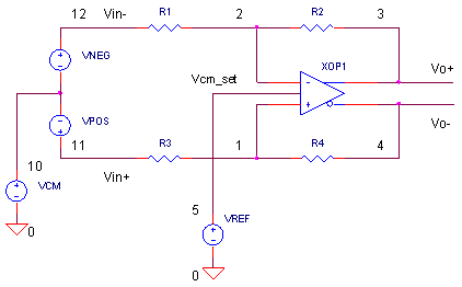
ADCIN_FULLY_DIFF1.CR Download the SPICE file
In this series of ADC input drivers, we've created differential outputs using the obvious - two op amps, one for the positive and one for the negative output. Also, you need 8 resistors to accomplish the feat. But, wouldn't it be grand if a single device produced with both positive and negative? Yes, as you might have guessed, the fully differential amplifier is the wonder device that makes your ADC driving challenges a little simpler. This single device with just 4 resistors can transform a single-ended or differential input into a differential output. Basically, it does the job of both the Single-Ended to Differential Output of Differential to Differential ADC Drivers.
TWO AMPS IN ONE
.The Fully Differential Amplifier actually has two internal amplifiers.
1. Differential Amplifier. This amp creates a differential output
Vod = (Vo+ - Vo-)
based on the inputs Vin+, Vin- and resistor values R1-R4.
2. Common-Mode Output Servo Amplifier. This amp sets the common-mode (or average) output voltage
Vcm_out = (Vo+ + Vo-) / 2
based on the voltage at its common-mode input pin, Vcm_set.
The servo amplifier adjusts the dc level of the output such that Vcm_out is equal to the Vcm_set pin. Cool! This is essential for shifting your differential output up or down, especially for a single-supply ADC that accepts a +/- 4V differential input centered around 2V.
THE BIG EQUATION
So how does this thing work? The answer lies in the equation that defines the input/outputs. I've seen the derivation of these equations. Oh my, its not your basic op amp circuit. After writing the nodal equations and much solving, setting, substituting, assuming, deriving, calculating, subtracting and simplifying, you get:
Vod = (Vo+ - Vo-)
= [ 2·{ Vin+
· (1-β1)
- Vin- · (1-β2) }
+ 2·Vcm_out·(β1-β2)
] / (β1+β2)
where
β1 = R1 / (R1+R2)
β2 = R3 / (R3+R4)
We see that the Vod is in terms of Vin+ and Vin- as expected. But oh nooooo - look what's appeared! The output common-mode level Vcm_out finds its way into the differential voltage too. Not good. However, as you can see, this equation can be further simplified by setting the resistor ratios equal, R2 / R1 = R4 / R3 = β1 = β2. Now, a simple equation falls out
Vod = (Vin+ - Vin-) · (1-β) / β
= (Vin+ - Vin-)
· R2 / R1
The output is terms of a simple R ratio and the Vcm_out term goes away. Yes, life is good - as long as you keep the ratios equal!
FULLY DIFF AMP IN ACTION
Let's test drive the fully differential amplifier with a ±2 V differential input creating a ±2 V differential output. For a gain of 1, we set R1 = R2 = R3 = R4 = 10 kΩ. Let's set the common-mode output level to 0V for now by setting VREF = 0V.
CIRCUIT INSIGHT Run a simulation of ADCIN_FULLY_DIFF1.CIR. Plot the inputs V(11) and V(12). In a separate window, plot both the positive and negative output, V(3) and V(4). For equal resistors and a ± 2V differential input, you should see outputs swing ±2 V differential! Finally, add the trace V(3)-V(4) to see the ± 2Vdifferential signal converted to ± 4Vsingle-ended signal. This signal-ended signal actually gets converted by the ADC typically mapping -4V to all 0s and +4V to all 1s.
HANDS-ON DESIGN Now suppose the ADC works from a single supply, +5 V and GND. In other words, negative input voltage can damage your ADC. The solution? Shift the Vcm_out of the differential amplifier by 2 V. Set VREF = 2.0 V and rerun the SPICE file. Any improvement? Yes, each differential output gets shifted by 2 V for differential swings between 0 and 4 V - safe within the maximum input levels of your ADC!
Suppose the input signal is only ±1V, but you still desire the full dynamic range of the ADC. Reduce the peak input signal to ±1V.
VPOS 11 10 SIN(0V +1VPEAK 1KHZ)
VNEG 12 10 SIN(0V -1VPEAK 1KHZ)
Choose resistor values for a gain of 2 and rerun your SPICE circuit. Did you achieve your ±2Vdifferential output?
RESISTOR MATCHING PART I - GAIN AND NOISE REJECTION
Not only does this circuit amplify differential signals, but it rejects common-mode signals. Any unwanted signals - DC offsets or noise - gets attenuated, passing only the differential signal. However, this gain and common-mode input rejection all depend on what? Notice that part of the differential output equation
Vin+ · (1-β1) - Vin- · (1-β2)
requires R2 / R1 = R4 / R3 = β1 = β2 = β so you can factor out (1-β) and get the difference.
(1-β1) ( Vin+ - Vin- )
Therefore, you need closely matched resistor ratios to get accurate gain and good rejection.
HANDS-ON DESIGN Let's inject a common-mode offset of 1 VDC and noise of 1 V at 10 kHz. Simply remove the comment character "*" before the statement
VCM 10 0 SIN(1.0 1VPEAK 10KHZ)
and place an "*" before the VCM statement that sets DC = 0 V. Rerun the simulation. Oh my, the inputs look awful corrupted by offset and noise. But, the fully differential amplifier saves the day! The outputs look squeaky clean as before.
Now let's throw this resistor matching grossly out of whack by setting R1 = 12 k and R3 = 10 k. Rerun the simulation. Is the output still from from offset and noise? No, the undesirables appear at the output! Not only that, but the gain has been reduced by 20%! The less undesirables and gain error you can tolerate at the output, the closer you need to match the resistor ratios.
RESISTOR MATCHING PART II - OUTPUT ERROR
Part of the differential output equation also contains the terms
2 · Vcm_out · (β1-β2)
Unfortunately, this tells you that the common-mode output voltage Vcm_out potentially makes its way into the differential output voltage! This term darkens our doorway because we want the differential output to be a function of Vin+ and Vin- only. Again, matching the resistor ratios R2 / R1 = R4 / R3 = β1 = β2 makes this term go away.
HANDS-ON DESIGN Set the differential inputs VPOS,VNEG and the common mode input VCM to 0V. Then set the VREF = 2V to set the common-mode output Vcm_out to 2V.
VPOS 11 10 SIN(0V +0VPEAK 1KHZ)
VNEG 12 10 SIN(0V -0VPEAK 1KHZ)
VCM 10 0 DC 0V
VREF 5 0 DC 2V
With R1 = R2 = R3 = R4 = 10 kΩ, run a simulation and plot the inputs V(11), V(12). In a separate window, plot the differential output V(3)-V(4). You should 0 V at the inputs and 0 V at the differential output. Life is good. But now, set R1 = 11 kΩ to throw off our resistor ratio matching by 10%. Rerun the simulation and check, V(3)-V(4). Life is not so good here. About 90 mV of error has entered the differential output due to Vcm_out = 2 V and a ratio mismatch.
Incrementally, tighten the ratio (R1 = 10.1, 10.01, 10.001 kΩ) and watch the gain tighten and the error shrink. What does this mean? Resistor tolerance and temperature coefficient are important if you require low errors in your application.
SINGLE-ENDED INPUTS
CIRCUIT INSIGHT Finally, you can convert single-ended signals to differential. Simply ground either the NEG input resistor R1 or the POS resistor R3. Let's ground R1, set the inputs to 2V and set the common-mode levels to 0V.
VPOS 11 10 SIN(0V +2VPEAK 1KHZ)
VNEG 12 10 SIN(0V -2VPEAK 1KHZ)
VCM 10 0 DC 0V
VREF 5 0 DC 0V
R1 0 2 10K
Run a simulation and plot the input V(12). In a separate window, plot both the positive and negative outputs V(3), V(4), and the differential output V(3)-V(4). What's differential here? Given a ±2 V single ended-input we get a ±2 V differential output - half of the output from a differential inputs. Also notice that each output V(3) or V(4) only needs to swing ±1 V to achieve the ±2 V differential output.
HANDS-ON DESIGN You can still add a common-mode out put voltage by setting VREF. However, if you add common-mode input noise and offset at VCM, these unwanted signals no longer get rejected. Try changing VREF and VCM. Then run a simulation to see its effect on the output.
FULLY DIFF AMP SUBCIRCUIT
Just a brief note about the subcircuit FULLYDIFF1. This is a very simple model with no frequency shaping components. So don't depend on this model to show you an accurate frequency response or if there's potential overshoot / ringing in a step response.
The Voltage-Controlled Voltage Sources EOUTP and EOUTN combine to create the differential output with an open-loop gain of 100000 V/V. ECM is the servo amplifier that drives the common connection of EOUP and EOUTN. This servo amp forces the average of the differential output (sampled by RCM1, RCM2) to equal the voltage you place at Vcm_set (pin 5). A good future topic might be a more complex Fully Differential Amplifier that includes frequency response.
MORE TOPICS
Here's around-up of the ADC driver topics to explore.
Single-Ended Input to Single-Ended Output
Differential Input to Single-Ended Output
Single-Ended Input to Differential Output
Differential Input to Differential Output
SIMULATION NOTES
For a more detailed description of the op amp, see the Basic
Op Amp
Model.
For a quick review of subcircuits, check out Why Use Subcircuits?
Get a crash course on SPICE simulation at
SPICE Basics.
A handy reference is available at SPICE
Command Summary.
Browse other circuits available from the Circuit
Collection page.
SPICE FILE
Download the file or copy this netlist into a text file with the *.cir extension.
ADCIN_FULLY_DIFF1.CIR - FULLY DIFFERENTIAL AMPLIFIER ADC DRIVER
*
* DIFFERENTIAL SOURCE
VPOS	11	10	SIN(0V	+2VPEAK	1KHZ)
VNEG	12	10	SIN(0V	-2VPEAK	1KHZ)
*
* COMMON MODE VOLTAGE
VCM	10	0	DC	0V
*VCM	10	0	SIN(0V	1VPEAK	10KHZ)
*
VREF	5	0	DC	0V
*
R1	12	2	10K
R2	2	3	10K
R3	11	1	10K
R4	1	4	10K
XOP1	1 2 3	4 5	FULLYDIFF1
*
*
* FULLY DIFF AMP MODEL ********************************
*                   vip vin vop von vcm_set
.SUBCKT FULLYDIFF1  1   2   3   4   5
* INPUT IMPEDANCE
RIN	1	2	10MEG
* OUTPUT VOLTAGES
EOUTP	3 7	VALUE = { V(1,2) * +100000/2 }
EOUTN	4 7	VALUE = { V(1,2) * -100000/2 }

* COMMON-MODE OUTPUT - SERVO AMP
ECM	7 0	5 6	1e6
RCM1	3	6	1MEG
RCM2	4	6	1MEG
RCMOUT	7	0	1MEG
RCMIN	5	0	1MEG
*
.ENDS
********************************************************
*
* ANALYSIS
.TRAN 	0.01MS  2MS
*
.PROBE
.END
© 2006 eCircuit Center