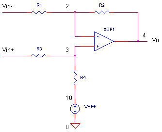
ADC Input Driver
SINGLE-ENDED
to SINGLE-ENDED
(Scale and Shift)
CIRCUIT
ADCIN_SE_SE1.CR Download the SPICE file
Suppose your sensor produces a bipolar voltage swing of ±10V. The only problem, your ADC accepts a single-ended input of 0 - 5 V. What you need is a circuit that will reduce your voltage swing. Not only that, you'll need to add an offset so your signal is positive only! The handy op amp circuit shown above, takes a single-ended input, then both scales and shifts it to a single-ended signal of your desires.
HOW IT WORKS
This circuit simply adds an input to the basic differential amplifier. You have two possible places you can connect your input signals: Vin+ or Vin-.
Now we've added an additional fixed input VREF to create an offset shift.
Now, how do you calculate Vo driven by all three sources? One easy way is by supersposition. Simply calculate Vo due to one source, with the other two sources set to zero. Then repeat for the other sources. Finally, add all of the outputs together.
| Input | Zero other inputs | Calc output | |
| Vin+ | Vin- =
0V VREF = 0V |
Vo1 =
Vin+ ∙R4/(R3+R4)∙(R1+R2)/R1 Assuming R2/R1 = R4/R3 we get Vo1 = Vin+ ∙ (R2/R1) |
|
| Vin- | Vin+ = 0V VREF = 0V |
Vo2 = Vin- ∙ (- R2/R1) | |
| VREF | Vin+ =
0V Vin- = 0V |
Vo3 =
VREF∙R3/(R4+R3) ∙ (R1+R2)/R1 Assuming R2/R1 = R4/R3 we get Vo3 = VREF |
The total output due to all sources Vin+, Vin- and VREF is the sum of the three outputs calculated above.
Vo = Vin+ ∙ (R2/R1) + Vin- ∙ (-R2/R1) + VREF
As you can see, the circuit fits our needs. The equation describes a function that applies a scaling factor R2/R1 to either input and adds an offset VREF.
SENSOR SIGNAL
Assuming the ±10 V sensor signal is the proper polarity, connect the sensor VS1 to the Vin+ input.
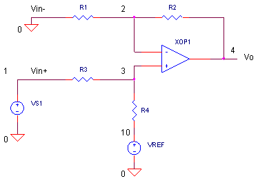
Recalling the 0 - 5V ADC input requirements, you need to scale down the 20Vp-p signal to a 5Vp-p input. This requires a scaling of 5/20=1/4. Given R2/R1 = 1/4 and selecting R1=R3=10k, you get R2=R4=2.5 k.
Now, your sensor signal is scaled from ±10 V to ±2.5 V. But how much offset, or VREF, should you add to force the signal to swing 0 - 5V? Yes, a shift of +2.5V should do the trick.
CIRCUIT INSIGHT Simulate the SPICE circuit ADCIN_SE_SE1.CIR. The initial circuit values are R1 = R2 =R3 = R4 = 10k and VREF = 0 V. Plot the signal V(1) and output V(4). Does V(1) get passed directly to V(4) with no scaling or offset?
Now set R2 = R4 = 2.5 kΩ and rerun the SPICE file. Did the ±10 V signal get scaled down by 1/4 to ±2.5 V? Finally, set VREF = 2.5 V and rerun the simulation. Does Vo get properly scaled and offset to create a 0 - 5 V ADC input as expected?
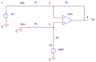
INVERTED SENSOR SIGNAL
Okay, your turn to design a circuit. Suppose a sensor creates an inverted sinewave that swings between 0 and 20V. However, your ADC accepts a bipolar ±5 V input. Basically, you need to invert, attenuate and shift the sensor signal before applying it to the ADC's input.
HANDS-ON DESIGN In the SPICE file, the new sensor signal is generated by VS2. To swap VS2 with VS1, remove the * before the VS2 statement and place an * in front of the VS1 statement. Your SPICE file should look like this.
*VS1 1 0 SIN(0V 10VPEAK
1KHZ)
VS2 1 0 SIN(10V -10VPEAK 1KHZ)
Next, the signal needs to be inverted, so you need to connect VS2 (node 1) to R1 (Vin-) and connect ground (node 0) to R3 (Vin+).
R1
1
2 10K
R2 2 4 10K
R3 0
3 10K
R4 3 10 10K
Set R1 = R2 =R3 = R4 = 10k and VREF = 0 V. Run a simulation and plot the signal V(1) and output V(4). You should V(1) get inverted properly to V(4) with no scaling or offset.
Here's your design challenge. What values of R1- R4 and VREF will
transform this inverted unipolar
0 - 20V signal to the bipolar
±5 V required at the ADC input?
MORE TOPICS
Here's around-up of the ADC driver topics to explore.
Single-Ended Input to Single-Ended Output
Differential Input to Single-Ended Output
Single-Ended Input to Differential Output
Differential Input to Differential Output
The last two functions require a couple of op amps. However, take a look at a single device - the Fully Differential Amplifier - that performs the functions.
SIMULATION NOTES
For a more detailed description of the op amp, see the Basic Op
Amp
Model.
For a quick review of subcircuits, check out Why Use Subcircuits?
Get a crash course on SPICE simulation at
SPICE Basics.
A handy reference is available at SPICE
Command Summary.
Browse other circuits available from the Circuit
Collection page.
SPICE FILE
Download the file or copy this netlist into a text file with the *.cir extension.
ADCIN_SE_SE1.CIR - SINGLE-ENDED TO SINGLE-ENDED ADC INPUT DRIVER
*

VS1	1	0	SIN(0V	10VPEAK	1KHZ)
*VS2	1	0	SIN(10V	-10VPEAK	1KHZ)
VREF	10	0	DC	0V
*
R1	0	2	10K
R2	2	4	10K
R3	1	3	10K
R4	3	10	10K
XOP1	3 2	4	OPAMP1
*
* SINGLE-POLE OPERATIONAL AMPLIFIER MACRO-MODEL
* connections:      non-inverting input
*                   |   inverting input
*                   |   |   output
*                   |   |   |
.SUBCKT OPAMP1	    1   2   6
* INPUT IMPEDANCE
RIN	1	2	10MEG
* DC GAIN (100K) AND POLE 1 (100HZ)
* GBWP = 10MHZ
EGAIN	3 0	1 2	100K
RP1	3	4	1K
CP1	4	0	1.5915UF
* OUTPUT BUFFER AND RESISTANCE
EBUFFER	5 0	4 0	1
ROUT	5	6	10
.ENDS
*
.TRAN 	0.01MS  2MS
*
.PLOT	TRAN 	V(1) V(4)
.PROBE
.END
© 2006 eCircuit Center