ADC Input Driver
DIFFERENTIAL to SINGLE-ENDED
CIRCUIT
ADCIN_DIFF_SE1.CR Download the SPICE file
Your data acquisition board has an ADC that accepts a single-ended input of 0 - 5 V. However, your signal source happens to be differential. This signal may be generated from a sensor bridge where one leg swings positive while the other swings negative in response to pressure, for example. Or, suppose noise corrupts both a remote signal and its local ground wire equally. Rejecting this common noise would clean up your desired signal.
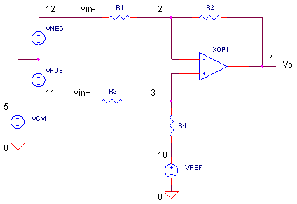
The Differential to Single-Ended ADC Driver would solve your design challenges. The op amp circuit shown above is remarkably similar to the Single-Ended to Single-Ended ADC Driver circuit covered previously. However, in this case we drive both inputs with the differential input. But, beware! the tolerance of the resistors you choose can make or break its performance!
HOW IT WORKS
From our previous analysis of the Single-Ended to Single-Ended driver (assuming R2/R1 = R4/R3), we got
Vo = Vin+ ∙ (R2/R1) + Vin- ∙ (-R2/R1) + VREF
which is really a differential receiver
Vo = [ Vin+ - Vin- ] ∙ (R2/R1) + VREF
In a nutshell, this circuit takes the difference of the inputs, applies a scaling factor of R2/R1 and adds an offset VREF.
SINGLE-ENDED AND DIFFERENTIAL REVIEW
A single-ended source generates a voltage between one node Vsig and a fixed reference, like ground.
A differential source generates a voltage between two output nodes, Vsig+ and Vsig-, neither one at ground potential!
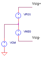
To find the output voltage, you measure the difference between the two nodes
Vdiff = Vsig+ - Vsig-
Typically one signal swings in the positive direction, while the other swings in the negative direction. As an example, let's say a differential source produces ± 4 V. This can be generated by VPOS producing a ± 2 V signal and VNEG producing an inverted ± 2 V signal. So max signals would be
Max positive signal: Vsig+ = +2V and Vsig- = -2V
Vdiff = 2-(-2) = +4 V.Max negative signal: Vsig+ = -2V and Vsig- = +2V
Vdiff = -2-(+2) = -4 V.
The average of the differential voltage is defined by the common-mode voltage represented by VCM.
A DIFFERENTIAL SENSOR
A remote sensor board produces a ±4 V
differential signal. Your ADC input requires a range of
0 - 5V. (You can think of a 0 - 5 V signal as being a
± 2.5 V signal with a 2.5V offset.)
This means you need to you reduce the ± 4 V
to ± 2.5 V signal. By how much? This factor is calculated
as 2.5 V / 4 V =
0.625 which also defines the R2 / R1 ratio. Selecting
R1 = R3 = 10 kΩ, you
get R2 = R4 = 6.25 kΩ.
Given the scaling alone, you expect your sensor signal to get attenuated from ± 4 V to ± 2.5 V. Obviously, you're not done yet. Add an offset, VREF = 2.5 V, to force the signal to swing 0 - 5V.
CIRCUIT INSIGHT Simulate the SPICE circuit ADCIN_DIFF_SE1.CIR. Start with these initial circuit values: R1 = R2 =R3 = R4 = 10k and VREF = 0 V. First check the basics. Plot inputs V(11), V(12) and the differential voltage by adding trace V(11)-V(12). Do you see ± 4 V differential? Now remove V(11)-V(12) and add the output and output V(4). Does the circuit find the difference between V(11) and V(12)? You should see the ± 4V at V(4) with no scaling or offset.
Now set R2 = R4 = 6.25 kΩ. Rerun the SPICE file. Did the ±4 V signal get scaled down to ±2.5 V? Finally, set VREF = 2.5 V and rerun the simulation. Does the circuit properly transform the differential input to a 0 - 5 V single-ended signal?
NOISE AND OFFSET
Okay, let's throw in some real world troubles (or challenges if you prefer). There's some 10 kHz noise getting on both the VPOS and VNEG lines. Also, the signal rides on top of a 2 V offset. You can simulate these effects by modifying the VCM statement.
VCM 5 0 SIN(2.0 1VPEAK 10KHZ)
CIRCUIT INSIGHT Rerun the SPICE file. Does the noise and offset at V(11) and V(12) get rejected by the circuit? Awesome, Cool, Wicked!
But, the rejection of noise and offset depends on perfectly matched resistor ratios: R2 / R1 = R4 / R3. Try changing R1 by 5%, say from 10k to 10.5 kΩ. Is the output signal still noise free? To get a better look, plot V(4) in a new plot window. Also, reduce VPOS and VNEG to 0.2 V and rerun the simulation. Do you see any noise slipping past the goalie?
Try reducing the tolerance of R1 to 1 %, or 10.1 kΩ. Did the noise get any smaller? Try replacing R1 with a 0.1% value or 10.01 kΩ. How much of the noise remains? As you can see, noise rejection is a direct function of how well the ratios are matched.
±10 DIFFERENTIAL SENSOR
Suppose you've got a new sensor that outputs ±10 V differential.
VPOS 11 5 SIN(0V +5VPEAK 1KHZ)
VNEG 12 5 SIN(0V -5VPEAK 1KHZ)
HANDS-ON DESIGN Start with these initial values: R1 = R2 =R3 = R4 = 10k and VREF = 0 V. What circuit values do you choose to transform the input into to a 0 - 5 V single-ended signal?
MORE TOPICS
Here's around-up of the ADC driver topics to explore.
Single-Ended Input to Single-Ended Output
Differential Input to Single-Ended Output
Single-Ended Input to Differential Output
Differential Input to Differential Output
The last two functions require a couple of op amps. However, take a look at a single device - the Fully Differential Amplifier - that performs the functions.
SIMULATION NOTES
For a more detailed description of the op amp, see the Basic
Op Amp
Model.
For a quick review of subcircuits, check out Why Use Subcircuits?
Get a crash course on SPICE simulation at
SPICE Basics.
A handy reference is available at SPICE
Command Summary.
Browse other circuits available from the Circuit
Collection page.
SPICE FILE
Download the file or copy this netlist into a text file with the *.cir extension.
ADCIN_DIFF_SE1.CIR - DIFFERENTIAL TO SINGLE-ENDED ADC INPUT DRIVER
*
* DIFFERENTIAL SOURCE
VPOS	11	5	SIN(0V	+2VPEAK	1KHZ)
VNEG	12	5	SIN(0V	-2VPEAK	1KHZ)
*
* COMMON MODE VOLTAGE
VCM	5	0	DC	0
*VCM	5	0	SIN(2.0V	1VPEAK	10KHZ)

*
VREF	10	0	DC	0V
*
R1	12	2	10K
R2	2	4	10K
*
R3	11	3	10K
R4	3	10	10K

XOP1	3 2	4	OPAMP1
*
* SINGLE-POLE OPERATIONAL AMPLIFIER MACRO-MODEL
* connections:      non-inverting input
*                   |   inverting input
*                   |   |   output
*                   |   |   |
.SUBCKT OPAMP1	    1   2   6
* INPUT IMPEDANCE
RIN	1	2	10MEG
* DC GAIN (100K) AND POLE 1 (100HZ)
* GBWP = 10MHZ
EGAIN	3 0	1 2	100K
RP1	3	4	1K
CP1	4	0	1.5915UF
* OUTPUT BUFFER AND RESISTANCE
EBUFFER	5 0	4 0	1
ROUT	5	6	10
.ENDS
*
.TRAN 	0.01MS  2MS
*
.PLOT	TRAN 	V(11) V(12) V(4)
.PRINT	TRAN 	V(11) V(12) V(4)
.PROBE
.END
© 2006 eCircuit Center