ADC Input Driver
DIFFERENTIAL to
DIFFERENTIAL
CIRCUIT
ADCIN_DIFF_DIFF1.CR Download the SPICE file
The last of our basic ADC input drivers is the differential input to differential output driver. Suppose another part of your circuit already converted a singled-ended sensor signal to ± 2Vdifferential. However, this differential signal sakes its way past noisy AC sources and switching power supplies. You've just a couple of tasks here: 1) Reject any common-mode noise that was picked up along the way to the ADC and 2) Shift the signals such that the differential signal is centered around 2 V (a typical requirement of a single-supply ADC input). As you've seen before, we can build from previous circuits. A couple of Differential to Single-Ended ADC Drivers should do the trick. The solution lies in properly connecting the differential inputs to get a non-inverting or inverting output.
A PAIR OF AMPS
Our building block is the Differential Input to Single-Ended ADC Driver. Assuming R2/R1 = R4/R3, we found the output to be
Vo = (Vin+ - Vin-) ∙ R2/R1 + VREF
Given the two differential input signals, VPOS and VNEG, take two amplifiers circuits and generate two outputs of opposite polarity.
Amplifier 1: Non-Inverting
Vo+ = (VPOS - VNEG) ∙ R2/R1 + VREF
Amplifier 2: Inverting
Vo- = (VNEG - VPOS) ∙ R2/R1 + VREF
All that's left is choosing the proper gain/attenuation (K = R2 / R1) for each amplifier and the offset (VREF).
HOW MUCH GAIN AND OFFSET?
For this example, all we're doing is taking a ± 2Vdifferential and creating a ± 2Vdifferential signal centered around 2V. Intuitively I thought all resistors would be the same value, say 10k. But I was surprised to find this answer was wrong! Why? Well, a differential to single ended amplifier (R1=R2=R3=R4) takes a ± 2Vdifferential input and generates a ± 4V single-ended output! Now, two of these amplifiers of opposite polarity creates a differential output of ± 4V. Twice as much as needed. Therefore, we'll include a factor of 1/2 in the gain equation.
For this example
K = ( ±2 V / ±2 V ) · 1/2
= 0.5 V/V
Choosing R2 = 10 kΩ, calculate R1 from the gain equation K = R2/R1
R1 = R2 · K
= 10 kΩ · 0.5
= 5 kΩ.
For an offset of 2 V, simply set VREF to this level.
TEST DRIVE
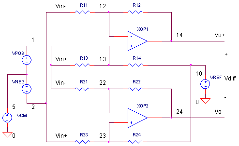
The SPICE file has two differential amplifiers XOP1 (with R11, R12, R13, R14) and XOP2 (with R21, R22, R23, R24) wired as a non-inverting and inverting amplifier, respectively. The gains are set by
K = R2 / R1
= R12 / R11 = R14 / R13
= R22 / R21 = R24 / R23
HANDS-ON DESIGN Start with these initial values: all Rs = 10k and VREF = 0 V. Run a simulation of ADCIN_SE_DIFF1.CIR. Plot the inputs V(1) and V(2). In a separate window, plot both the positive and negative output, V(14) and V(24). For equal resistors and a ± 2Vdifferential input, you should see outputs swing ±4 V differential! This was the initial surprise I spoke of earlier.
Now adjust the individual amplifier gain to 0.5 by changing R12 = R14 = R22 = R24 = 5 k. Rerun the simulation and check the differential output. Okay, now you've got the desired ± 2Vdifferential. BUT, each output swings positive and negative! Not good for an ADC that runs from a single +5 V supply.
Now set VREF = 2.0 V and rerun the SPICE file. Any improvement? Yes, each output gets shifted by 2 V for a total swing between 0 and 4 V. Good news for the ADC input!
COMMON-MODE NOISE
The ADC has a differential input which has the ability to reject common-mode offsets and noise. However, the common-mode range usually has serious limitations of GND and the 5V supply. Your op amp differential amplifier has a much wider common mode range, especially if you can run it from wider supply rails.
Suppose your signal gets corrupted by some 10 kHz noise getting on both the VPOS and VNEG lines. Also, the signal rides on top of a 2 V offset. You can simulate these effects by modifying the VCM statement.
VCM 5 0 SIN(1.0 1VPEAK 10KHZ)
CIRCUIT INSIGHT Rerun the SPICE file. Does the noise and offset at V(1) and V(2) get rejected by at the output V(14) and V(24)! Yes, the circuit is a success! To get a better view of the rejection, suppress the input signal.
VPOS 1 5 SIN(0V +0VPEAK 1KHZ)
VNEG 2 5 SIN(0V -0VPEAK 1KHZ)
Run a new simulation. The amount of 10 kHz that squeaks through should be small. But remember, rejection of noise and offset depends on perfectly matched resistor ratios: R2 / R1 = R4 / R3. Try changing a resistor by 5%, say from 10k to 10.5 kΩ. What happens to level of the 10 kHz noise at the output?
MANY PATHS
The circuits covered in this ADC driver series are just a few examples of how to get the job done. Just visit a few op amp manufacturer's websites and you're bound to see a different way to drive ADC's. There are many methods and each have their advantages: low-noise, low drift, low-cost, high bandwidth, etc. No easy answers. You just have to roll up your sleeves, analyze their performance and make the best choice you can.
MORE TOPICS
Here's around-up of the ADC driver topics to explore.
Single-Ended Input to Single-Ended Output
Differential Input to Single-Ended Output
Single-Ended Input to Differential Output
Differential Input to Differential Output
The last two functions require a couple of op amps. However, take a look at a single device - the Fully Differential Amplifier - that performs the functions.
SIMULATION NOTES
For a more detailed description of the op amp, see the Basic
Op Amp
Model.
For a quick review of subcircuits, check out Why Use Subcircuits?
Get a crash course on SPICE simulation at
SPICE Basics.
A handy reference is available at SPICE
Command Summary.
Browse other circuits available from the Circuit
Collection page.
SPICE FILE
Download the file or copy this netlist into a text file with the *.cir extension.
ADCIN_DIFF_DIFF1.CIR - DIFFERENTIAL TO DIFFERENTIAL ADC INPUT DRIVER
*
* DIFFERENTIAL SOURCE
VPOS	1	5	SIN(0V	+2VPEAK	1KHZ)
VNEG	2	5	SIN(0V	-2VPEAK	1KHZ)
*
* COMMON MODE VOLTAGE
VCM	5	0	DC	0V
*VCM	5	0	SIN(1.0V	1VPEAK	10KHZ)
*
VREF	10	0	DC	0V
*
* NON-INVERTING OUTPUT
R11	2	12	10K
R12	12	14	10K
R13	1	13	10K
R14	13	10	10K
XOP1	13 12	14	OPAMP1
*
* INVERTING OUTPUT
R21	1	22	10K
R22	22	24	10K
R23	2	23	10K
R24	23	10	10K
XOP2	23 22	24	OPAMP1
*
*
* SINGLE-POLE OPERATIONAL AMPLIFIER MACRO-MODEL
* connections:      non-inverting input
*                   |   inverting input
*                   |   |   output
*                   |   |   |
.SUBCKT OPAMP1	    1   2   6
* INPUT IMPEDANCE
RIN	1	2	10MEG
* DC GAIN (100K) AND POLE 1 (100HZ)
* GBWP = 10MHZ
EGAIN	3 0	1 2	100K
RP1	3	4	1K
CP1	4	0	1.5915UF
* OUTPUT BUFFER AND RESISTANCE
EBUFFER	5 0	4 0	1
ROUT	5	6	10
.ENDS
*
.TRAN 	0.01MS  2MS
*
.PROBE
.END
© 2006 eCircuit Center